BD6973FV-LBE2 데이터 시트보기 (PDF) - ROHM Semiconductor
부품명
상세내역
일치하는 목록
BD6973FV-LBE2 Datasheet PDF : 20 Pages
| |||
BD6973FV-LB
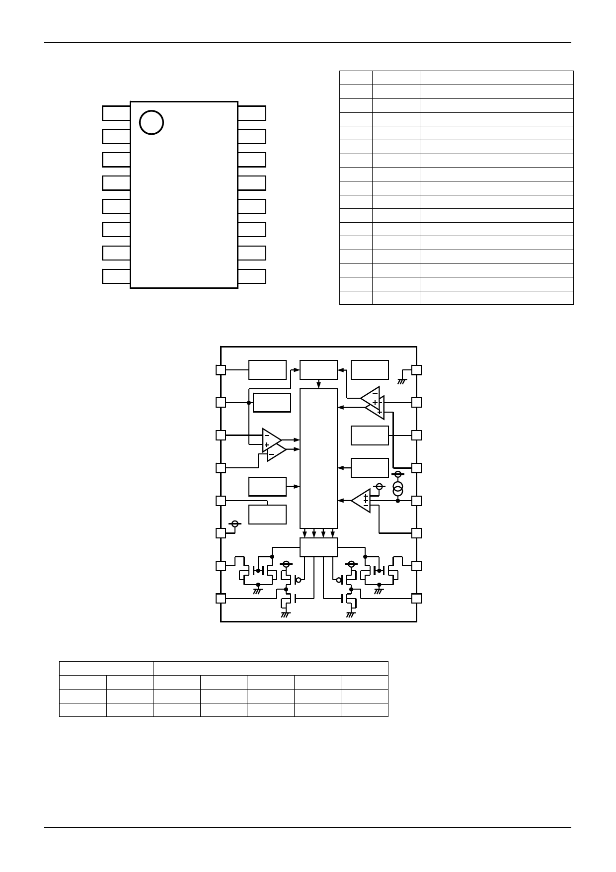
Pin Configuration
FG 1
OSC 2
MIN 3
TH 4
REF 5
Vcc 6
A1H 7
A1L 8
(TOP VIEW)
16 GND
15 H–
14 HB
13 H+
12 SS
11 CS
10 A2H
9 A2L
Figure 1. Pin Configuration
Block Diagram
Datasheet
Pin Description
P/No. P/Name
1
FG
2
OSC
3
MIN
4
TH
5
REF
6
Vcc
7
A1H
8
A1L
9
A2L
10
A2H
11
CS
12
SS
13
H+
14
HB
15
H–
16
GND
Function
Speed pulse signal output pin
Oscillating capacitor connecting pin
Minimum output duty setting pin
Output duty controllable input pin
Reference voltage output pin
Power supply pin
High side output 1 pin
Low side output 1 pin
Low side output 2 pin
High side output 2 pin
Output current detection pin
Soft start capacitor connecting pin
Hall + input pin
Hall bias pin
Hall – input pin
Ground pin
1 FG
2 OSC
3 MIN
TH
4
5 REF
Vcc
6
Vcc
A1 H
7
SIGNAL
OUTPUT
PWM SOFT
SWITCHING
TSD
GND 16
OSC
PWM
COMP
H AL L
AMP
H AL L
COMP
HALL
BIAS
H– 15
HB 14
PWM
COMP
CONTROL
LOGIC
QUICK
START
LOCK
PROTECT
Vcl
REF
REG
SOFT START
& CURRENT
LIMIT COMP
PRE-
DRIVER
REG
H+
13
12
SS
CS 11
A2 H
10
8 A1L
A2L 9
I/O Truth Table
Hall Input
H+
H–
A1H
H
L
Hi-Z
L
H
L
H; High, L; Low, Hi-Z; High impedance
FG output is open-drain type.
Figure 2. Block Diagram
Driver Output
A1L
A2H
A2L
FG
H
L
L
Hi-Z
L
Hi-Z
H
L
www.rohm.com
© 2013 ROHM Co., Ltd. All rights reserved.
TSZ22111・15・001
2/17
TSZ02201-0H1H0B100820-1-2
27.Feb.2014 Rev.002
Share Link: 