MC33163 데이터 시트보기 (PDF) - Motorola => Freescale
부품명
상세내역
일치하는 목록
MC33163 Datasheet PDF : 16 Pages
| |||
Order this document by MC34163/D
Power Switching Regulators
The MC34163 series are monolithic power switching regulators that
contain the primary functions required for dc–to–dc converters. This series is
specifically designed to be incorporated in step–up, step–down, and
voltage–inverting applications with a minimum number of external
components.
These devices consist of two high gain voltage feedback comparators,
temperature compensated reference, controlled duty cycle oscillator, driver
with bootstrap capability for increased efficiency, and a high current output
switch. Protective features consist of cycle–by–cycle current limiting, and
internal thermal shutdown. Also included is a low voltage indicator output
designed to interface with microprocessor based systems.
These devices are contained in a 16 pin dual–in–line heat tab plastic
package for improved thermal conduction.
• Output Switch Current in Excess of 3.0 A
• Operation from 2.5 V to 40 V Input
• Low Standby Current
• Precision 2% Reference
• Controlled Duty Cycle Oscillator
• Driver with Bootstrap Capability for Increased Efficiency
• Cycle–by–Cycle Current Limiting
• Internal Thermal Shutdown Protection
• Low Voltage Indicator Output for Direct Microprocessor Interface
• Heat Tab Power Package
MC34163
MC33163
POWER SWITCHING
REGULATORS
SEMICONDUCTOR
TECHNICAL DATA
16
1
P SUFFIX
PLASTIC PACKAGE
CASE 648C
(DIP–16)
16
1
DW SUFFIX
PLASTIC PACKAGE
CASE 751G
(SOP–16L)
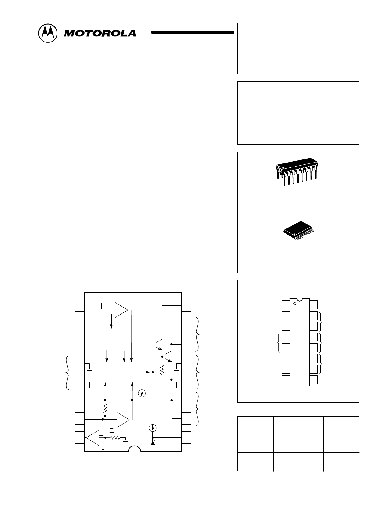
Representative Block Diagram
Ipk Sense 8
VCC 7
Timing
Capacitor
6
– ILimit
+
+
OSC
9
Driver
Collector
10
Switch
Collector
11
5
Gnd
4
Control Logic
and Thermal
Shutdown
+
12
Gnd
13
Voltage
Feedback 1
3
Voltage
Feedback 2
2
VFB
+
+
–
LVI
LVI Output 1
+
+
–
+
14
Switch
Emitter
15
16
Bootstrap
Input
(Bottom View)
This device contains 114 active transistors.
MOTOROLA ANALOG IC DEVICE DATA
PIN CONNECTIONS
LVI Output 1
Voltage Feedback 2 2
Voltage Feedback 1 3
4
Gnd
5
Timing Capacitor 6
VCC 7
Ipk Sense 8
16 Bootstrap Input
15 Switch
14 Emitter
13
Gnd
12
11
Switch Collector
10
9 Driver Collector
(Top View)
ORDERING INFORMATION
Device
Operating
Temperature Range Package
MC34163DW
MC34163P
TA = 0° to +70°C
SOP–16L
DIP–16
MC33163DW
MC33163P TA = – 40° to +85°C
SOP–16L
DIP–16
© Motorola, Inc. 1996
Rev 2
1
Share Link: 