DAP011 데이터 시트보기 (PDF) - ON Semiconductor
부품명
상세내역
일치하는 목록
DAP011 Datasheet PDF : 24 Pages
| |||
DAP011/DAP011C
latch
reset
2V
0V
ON
20k
Rcomp
LEB
CS
Rsense
from FB
setpoint
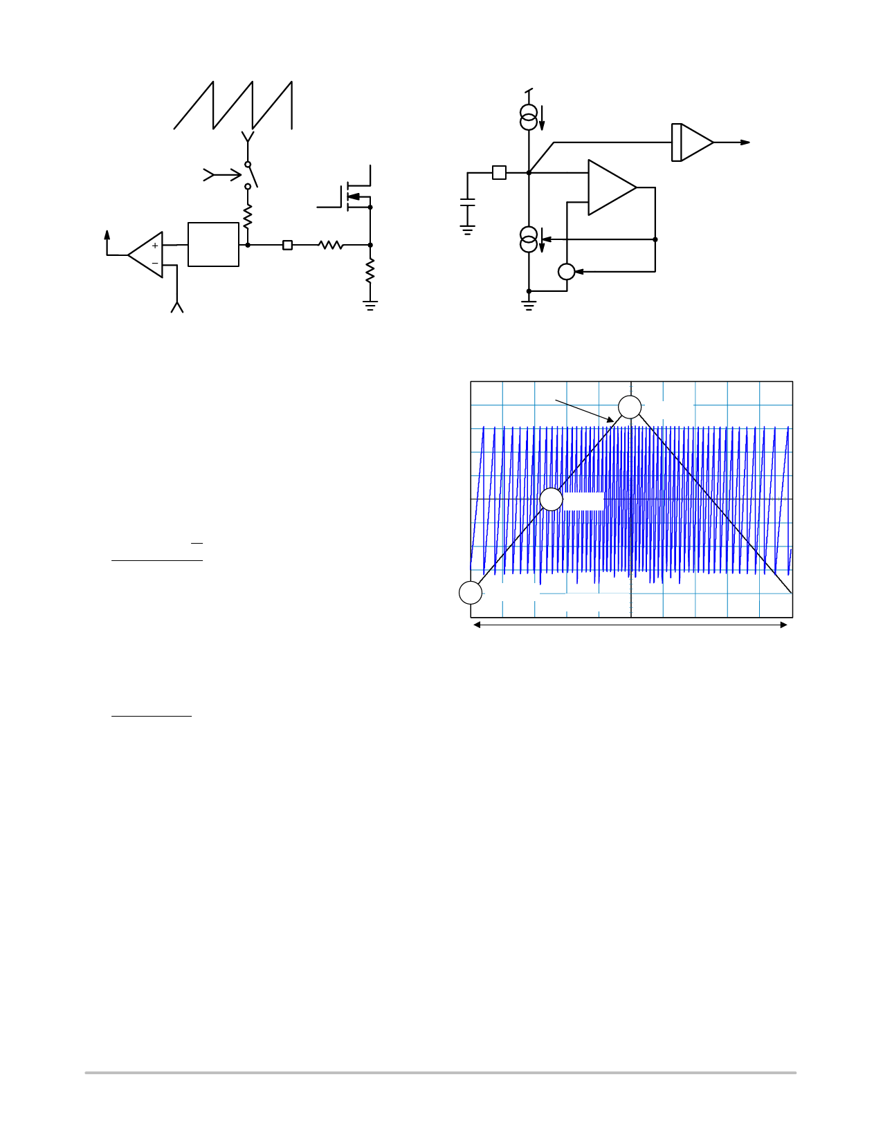
Figure 33. Inserting a resistor in series with the
current sense information brings ramp compensation
and stabilizes the converter in CCM operation
In the Speedking, the oscillator ramp features a 2.0 V
swing. If our clock operates at a 65 kHz pace, then the
oscillator slope corresponds to a 130 mV/ms ramp. In our
FLYBACK design, let’s assume that our primary inductance
Lp is 350 mH, and the SMPS delivers 12 V with a Np:Ns ratio
of 1:0.1. The OFF time primary current slope is thus given
by:
(Vout
)
Vf)
@
Ns
Np
+ 371 mAńms or 37 mVńms
Lp
(eq. 2)
When projected over an Rsense of 0.1 W, for instance. If we
select 75% of the downslope as the required amount of ramp
compensation, then we shall inject 27 mV/ms. Our internal
compensation being of 130 mV, the divider ratio (divratio)
between Rcomp and the 20 kW is 0.207. A few lines of
algebra to determine Rcomp:
20 k @ divratio + 5.2 kW
(1 * divratio)
(eq. 3)
Frequency Jittering
Frequency jittering is a method used to soften the EMI
signature by spreading the energy in the vicinity of the main
switching component. Speedking offers a ±5% (±6% for
DAP011C) deviation of the nominal switching frequency.
The sweep sawtooth is internally generated and modulates
the clock up and down with an adjustable period. Figure 34
displays the internal arrangement around Pin 4. It is actually
a I – 2I generator, producing a clean 50% duty−cycle
sawtooth. If we take a 1.4 V swing on the jitter capacitor,
then we calculate the needed value for a 3 ms period, or a 330
Hz modulation speed, again applying the V x C = I x t
relationship. We need 1.5 ms to ramp−up and 1.5 ms to ramp
down, therefore: C = 20u x 1.5m / 1.4 = 21 nF. If we select
a 22 nF, then our modulation frequency will be around
325 Hz. Figure 35 shows the relationship between the jitter
ramp and the frequency deviation.
VDD
iCjit
Jitter
4
Ctimer
Frequency
modulation
+
−
to clock
circuit
2.iCjit
+
VCjitP
VCjitV
Figure 34. An Internal Ramp is used to introduce
Frequency Jittering on the Oscillator Sawtooth
Jitter
ramp
68.9 kHz
65kHz
61.1 kHz
Adjustable
Internal
sawtooth
Figure 35. Modulation Effects on the Clock Signal by
the Jittering Sawtooth
Skipping Cycle Mode
Speedking automatically skips switching cycles when the
output power demand drops below a given level. This is
accomplished by monitoring the FB pin. In normal
operation, Pin 5 imposes a peak current accordingly to the
load value. If the load demand decreases, the internal loop
asks for less peak current. When this setpoint reaches a fixed
determined level, the IC prevents the current from
decreasing further down and starts to blank the output
pulses. The IC enters the so−called skip cycle mode, also
named controlled burst operation. The default skip cycle
current is internally frozen to 30% of the maximum peak
current which is 350 mV/Rsense The power transfer now
depends upon the width of the pulse bunches (Figure 38).
Suppose we have the following component values:
Primary Inductance (Lp) = 350 mH
Switching Frequency (Fsw) = 65 kHz
Ip skip = 600 mA (or 350 mV / Rsense)
The theoretical power transfer is therefore:
http://onsemi.com
20
Share Link: 