P1014AP100G 데이터 시트보기 (PDF) - ON Semiconductor
부품명
상세내역
일치하는 목록
P1014AP100G Datasheet PDF : 23 Pages
| |||
NCP1010, NCP1011, NCP1012, NCP1013, NCP1014
PIN FUNCTION DESCRIPTION
Pin No.
(SOT−223)
Pin No.
(PDIP−7)
Pin Name
Function
Description
1
1
VCC
Powers the Internal Circuitry This pin is connected to an external capacitor of typic-
ally 10 mF. The natural ripple superimposed on the
VCC participates to the frequency jittering. For im-
proved standby performance, an auxiliary VCC can be
connected to Pin 1. The VCC also includes an active
shunt which serves as an opto fail−safe protection.
−
2
NC
−
−
−
3
GND
The IC Ground
−
2
4
FB
Feedback Signal Input
By connecting an optocoupler to this pin, the peak
current setpoint is adjusted accordingly to the output
power demand.
3
5
Drain
Drain Connection
The internal drain MOSFET connection.
−
−
−
−
−
−
7
GND
The IC Ground
−
4
8
GND
The IC Ground
−
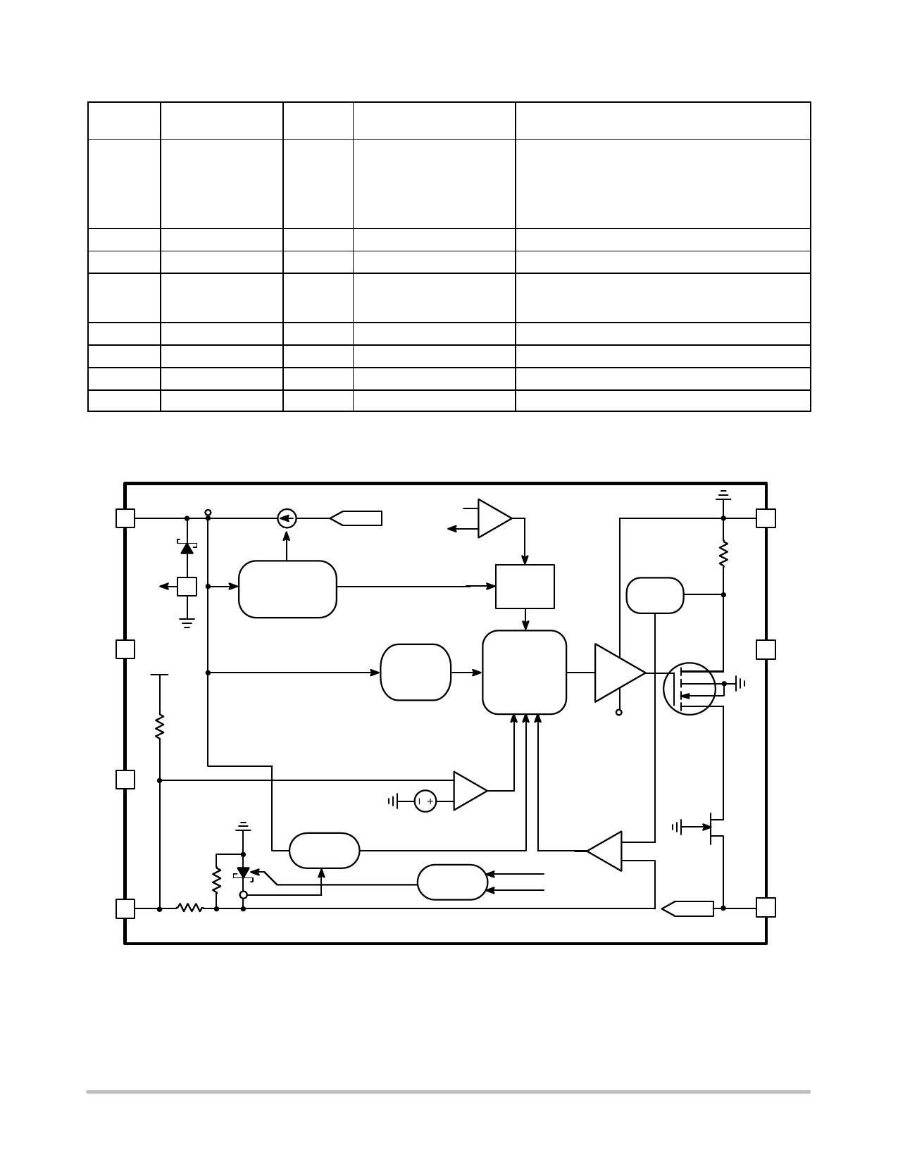
VCC 1
VCC
Vclamp*
IVCC
I?
Startup Source
Iref = 7.4 mA −
Drain
IVCC
+
UVLO
Management
High when VCC t 3 V
S
R
Q
Rsense
250 ns
L.E.B.
NC 2
4V
EMI Jittering
GND 3
18 k
Error flag armed?
FB 4
Overload?
65, 100 or
130 kHz
Clock
Reset
Set Flip−Flop Q
DCmax = 65%
Reset
Driver
VCC
−
+
0.5 V
+
Startup Sequence -
Soft−Start Overload
Drain
*Vclamp = VCCOFF + 200 mV (8.7 V Typical)
Figure 2. Simplified Internal Circuit Architecture
8 GND
7 GND
5 Drain
http://onsemi.com
3
Share Link: 