NJW1136D 데이터 시트보기 (PDF) - Japan Radio Corporation
부품명
상세내역
일치하는 목록
NJW1136D Datasheet PDF : 31 Pages
| |||
NJW1136
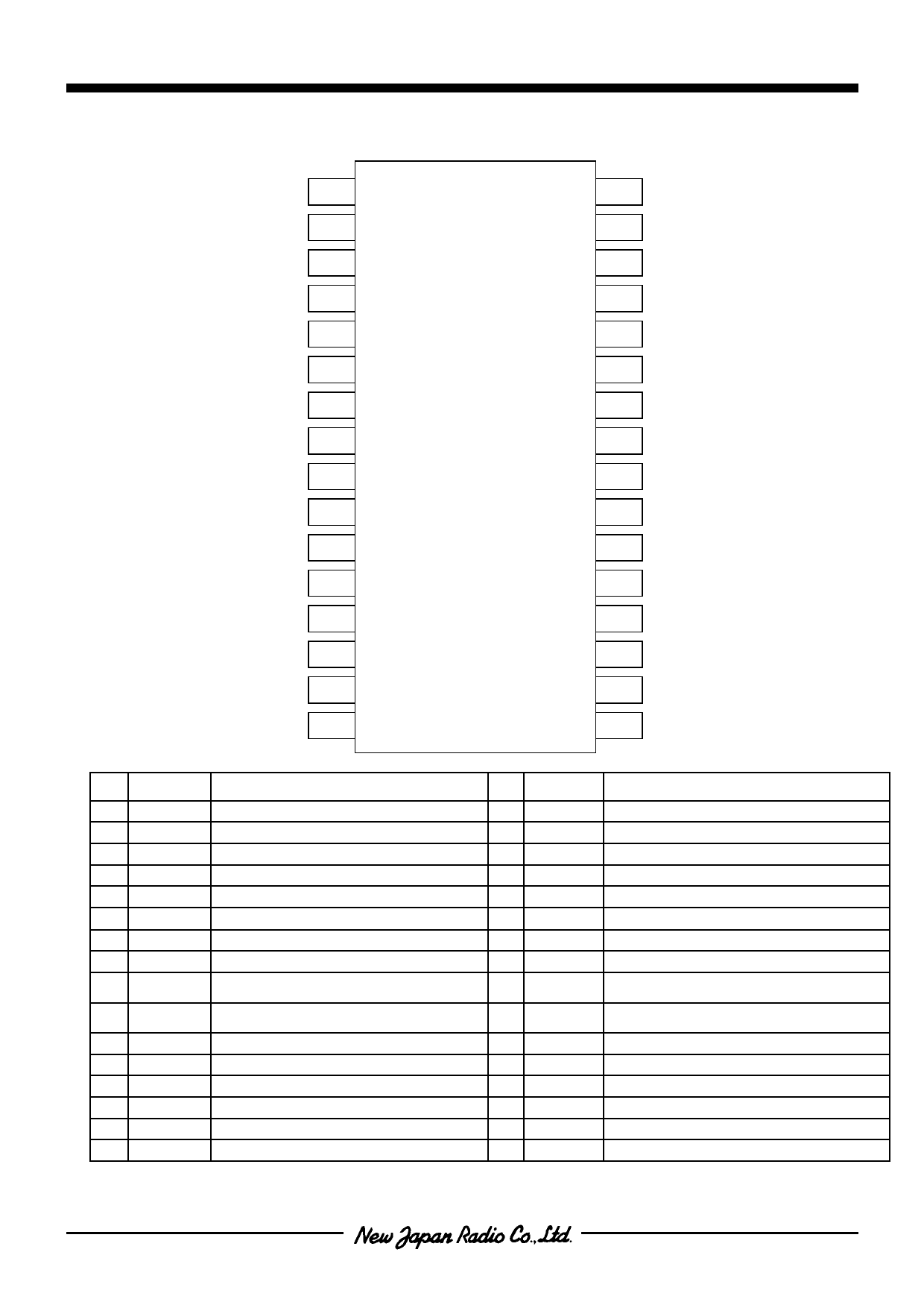
!PIN CONFIGURATION
1 INa
2 SR-FIL
3 SS-FIL
4 TONE-Ha
5 TONE-La
6 OUTW
7 OUTa
8 AGC1
9 AUX0
10 AUX1
11 PORT0
12 PORT1
13 ADR
14 SDA
15 SCL
16 GND
INb 32
LF1 31
LF2 30
LF3 29
TONE-Hb 28
TONE-Lb 27
OUTb 26
AGC2 25
CVA 24
CVB 23
CVW 22
CTH 21
CTL 20
CSR 19
Vref 18
V+ 17
No. Symbol
Function
No. Symbol
Function
1
INa
Ach input terminal
17
V+
Supply voltage terminal
2
SR-FIL Surround filter terminal
18
Vref
Reference voltage terminal
3
SS-FIL Simulated stereo filter terminal
19
CSR
DAC output terminal for surround control
4
TONE-Ha Ach tone control (treble) filter terminal
20
CTL
DAC output terminal for tone control (bass)
5
TONE-La Ach tone control (bass) filter terminal
21
CTH
DAC output terminal for tone control (treble)
6
OUTw Subwoofer output terminal
22
CVW
Bch DAC output terminal for LPF trimmer
7
OUTa
Ach output terminal
23
CVB
Bch DAC output terminal for volume and balance
8
AGC1 AGC attack and recovery time setting terminal 24
CVA
Ach DAC output terminal for volume and balance
9
AUX0(#)
Auxiliary 3 values voltage output terminal
(0.0V, 2.5V, 5V)
10
AUX1
Auxiliary 2 values voltage output terminal
(0.0V, V+)
25
AGC2 AGC boost level setting terminal
26
OUTb Bch output terminal
11
PORT0 Logic input terminal
27 TONE-Lb Bch tone control (bass) filter terminal
12
PORT1 Logic input terminal
28 TONE-Hb Bch tone control (treble) filter terminal
13
ADR
Slave address setting terminal
14
SDA
I2C data terminal
15
SCL
I2C cock terminal
29
LF3
LPF filter3 terminal
30
LF2
LPF filter2 terminal
31
LF1
LPF filter1 terminal
16
GND
Ground terminal
32
INb
Bch input terminal
(#) The AUX0 terminal should be connected via the protection resistance to 5V device.
(2/2)
Share Link: 