LV11961HA-AH 데이터 시트보기 (PDF) - ON Semiconductor
부품명
상세내역
일치하는 목록
LV11961HA-AH Datasheet PDF : 18 Pages
| |||
LV11961HA
Specifications
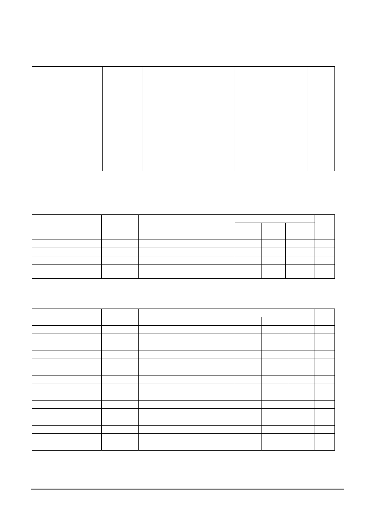
Absolute Maximum Ratings at Ta = 25C (Note 1)
Parameter
Symbol
Conditions
Ratings
Unit
Power supply voltage
VCCmax
18
V
Output pin current
IOUTmax
1.0
A
Output pin peak current
IOpeak max
Duty ≤ 10%
1.2
A
Output pin with stand voltage
VOUTmax
18
V
REG output maximum current
IREGmax
10
mA
HB output maximum current
IHBmax
10
mA
VTH pin voltage
VTHmax
4
V
FG/RG output pin voltage
VFG/VRDmax
18
V
FG/RG pin sink current
IFG/IRDmax
10
mA
Allowable power dissipation
Pdmax
Mounted on specified board (Note 2)
1.1
W
Operating temperature
Topr
(Note 3)
–40 to +95
C
Storage temperature
Tstg
–55 to +150
C
1.Stresses exceeding those listed in the Absolute Maximum Rating table may damage the device. If any of these limits are exceeded, device functionality
should not be assumed, damage may occur and reliability may be affected.
2. Specified board: 114.3mm x 76.1mm x 1.6mm, glass epoxy board
3. Do not exceed Tjmax=150C
Recommendation Operating Condition at Ta = 25C (Note 4)
Parameter
Operating supply voltage range
Symbol
VCCop
Conditions
min
3.6
Ratings
typ
12
Unit
max
16
V
VTH pin input voltage range
VTHop
0
VREG
V
RMI pin input voltage range
VRMlop
0
VREG
V
IN1/IN2 pin input voltage range VICM
0.2
VREG–1.2
V
CPWM pin oscillation frequency fCPWM
20
100 kHz
range
4. Functional operation above the stresses listed in the Recommended Operating Ranges is not implied. Extended exposure to stresses
beyond the Recommended Operating Ranges limits may affect device reliability.
Electrical Characteristics at Ta 25C, VCC = 12V (Note 5)
Parameter
Symbol
Conditions
Circuit current
REG pin voltage
HB pin voltage
CPWM pin high threshold level
CPWM pin low threshold level
CPWM amplitude
CPWM pin charge current
CPWM pin discharge current
SFS pin charge current
SFS pin clamp voltage
Sensitivity to hall input
OUT pin low level voltage
OUT pin high level voltage
FG/RD pin low level voltage
FG/RD pin leak current
ICC
VREG
VHB
VCPH
VCPL
DVCP
ICPWM
ICPWM
ISFS
VSFSCL
VHIN
VOL
VOH
VFGL/VRDL
IFGL/IRDL
IREG=5mA
IHB=5mA
VCPWM=1.4V
VCPWM=1.4V
Design target (Note 6)
IOUT=200mA
IOUT=200mA
IOUT=3mA
VFG/VRD=18V
min
2.80
1.08
2.05
0.57
1.41
19
–32
0.75
0.2
Ratings
typ
2.0
3.15
1.2
2.15
0.62
1.53
24
–24
1.25
0.4
10
0.11
0.18
0.1
Unit
max
3.0 mA
3.50
V
1.32
V
2.25
V
0.67
V
1.65
V
32 A
–19 A
1.85 A
0.6
V
20 mV
0.17
V
0.27
V
0.2
V
10 A
Continued on next page
www.onsemi.com
2
Share Link: 