MAX1203ACAP 데이터 시트보기 (PDF) - Maxim Integrated
부품명
상세내역
일치하는 목록
MAX1203ACAP Datasheet PDF : 24 Pages
| |||
MAX1202/MAX1203
5V, 8-Channel, Serial, 12-Bit ADCs
with 3V Digital Interface
Absolute Maximum Ratings
VDD to GND.............................................................-0.3V to +6V
VL.............................................................. -0.3V to (VDD + 0.3V)
VSS to GND..............................................................+0.3V to -6V
VDD to VSS.............................................................-0.3V to +12V
CH0–CH7 to GND.......................... (VSS - 0.3V) to (VDD + 0.3V)
CH0–CH7 Total Input Current...........................................±20mA
REF to GND.............................................. -0.3V to (VDD + 0.3V)
REFADJ to GND........................................ -0.3V to (VDD + 0.3V)
Digital Inputs to GND................................ -0.3V to (VDD + 0.3V)
Digital Outputs to GND................................. -0.3V to (VL + 0.3V)
Digital Output Sink Current.................................................25mA
Continuous Power Dissipation (TA = +70°C)
PDIP (derate 11.11mW/°C above +70°C).....................889mW
SSOP (derate 8.00mW/°C above +70°C).....................640mW
Operating Temperature Ranges
MAX1202_C_P/MAX1203_C_P...........................0°C to +70°C
MAX1202_E_P/MAX1203_E_P....................... -40°C to +85°C
Storage Temperature Range............................. -60°C to +150°C
Lead Temperature (soldering, 10s).................................. +300°C
Soldering Temperature (reflow)........................................+260°C
Stresses beyond those listed under “Absolute Maximum Ratings” may cause permanent damage to the device. These are stress ratings only, and functional operation of the device at these
or any other conditions beyond those indicated in the operational sections of the specifications is not implied. Exposure to absolute maximum rating conditions for extended periods may affect
device reliability.
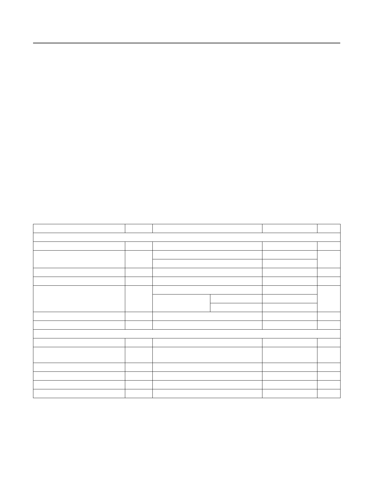
Electrical Characteristics
(VDD = +5V ±5%, VL = 2.7V to 3.6V; VSS = 0V or -5V ±5%; fSCLK = 2.0MHz, external clock (50% duty cycle); 15 clocks/conversion
cycle (133ksps); MAX1202—4.7μF capacitor at REF pin; MAX1203—external reference, VREF = 4.096V applied to REF pin; TA = TMIN
to TMAX, unless otherwise noted.)
PARAMETER
DC ACCURACY (Note 1)
Resolution
Relative Accuracy (Note 2)
Differential Nonlinearity
SYMBOL
CONDITIONS
RES
INL
DNL
MAX1202A/MAX1203A
MAX1202B/MAX1203B
no missing codes over temperature
MIN TYP MAX UNITS
12
Bits
±0.5
LSB
±1.0
±1.0 LSB
Offset Error
Gain Error (Note 3)
Gain Temperature Coefficient
MAX1202 (all grades)
External reference,
4.096V
MAX1203A
MAX1203B
External reference, 4.096V
±3.0 LSB
±3
±1.5 LSB
±3
±0.8
ppm/°C
Channel-to-Channel Offset Matching
±0.1
LSB
DYNAMIC SPECIFICATIONS (10kHz sine-wave input, 4.096VP-P, 133ksps, 2.0MHz external clock, bipolar-input mode)
Signal-to-Noise Plus Distortion Ratio SINAD
70
dB
Total Harmonic Distortion (up to the
5th Harmonic)
THD
-80
dB
Spurious-Free Dynamic Range
Channel-to-Channel Crosstalk
Small-Signal Bandwidth
Full-Power Bandwidth
SFDR
VIN = 4.096VP-P, 65kHz (Note 4)
-3dB rolloff
80
-85
4.5
800
dB
dB
MHz
kHz
www.maximintegrated.com
Maxim Integrated │ 2
Share Link: 