74LV595D(2016) 데이터 시트보기 (PDF) - NXP Semiconductors.
부품명
상세내역
일치하는 목록
74LV595D
(Rev.:2016)
(Rev.:2016)
NXP Semiconductors.

74LV595D Datasheet PDF : 20 Pages
| |||
Nexperia
74LV595
8-bit serial-in/serial-out or parallel-out shift register; 3-state
Table 7. Dynamic characteristics …continued
Voltages are referenced to GND (ground = 0 V). For test circuit see Figure 13.
Symbol Parameter
Conditions
40 C to +85 C
Min Typ[1] Max
fmax
maximum
frequency
SHCP or STCP; see Figure 8
and Figure 9
VCC = 2.0 V
14.0 40.0
-
VCC = 2.7 V
19.0 58.0
-
VCC = 3.3 V; CL = 15 pF
-
77
-
VCC = 3.0 V to 3.6 V
[3] 24.0 70.0
-
CPD
power dissipation VI = GND to VCC; VCC = 3.0 V [7] -
115
-
capacitance
40 C to +125 C Unit
Min
Max
12
-
MHz
16
-
MHz
-
-
MHz
20
-
MHz
-
-
pF
[1] Typical values are measured at Tamb = 25 C.
[2] tpd is the same as tPLH and tPHL.
[3] Typical value measured at VCC = 3.3 V.
[4] ten is the same as tPZH and tPZL.
[5] tdis is the same as tPHZ and tPLZ.
[6] Skew between any two outputs of the same package switching in the same direction. This parameter is guaranteed by design.
[7] CPD is used to determine the dynamic power dissipation (PD in W).
PD = CPD VCC2 fi N + (CL VCC2 fo) where:
fi = input frequency in MHz;
fo = output frequency in MHz;
CL = output load capacitance in pF;
VCC = supply voltage in V;
N = number of inputs switching;
(CL VCC2 fo) = sum of outputs.
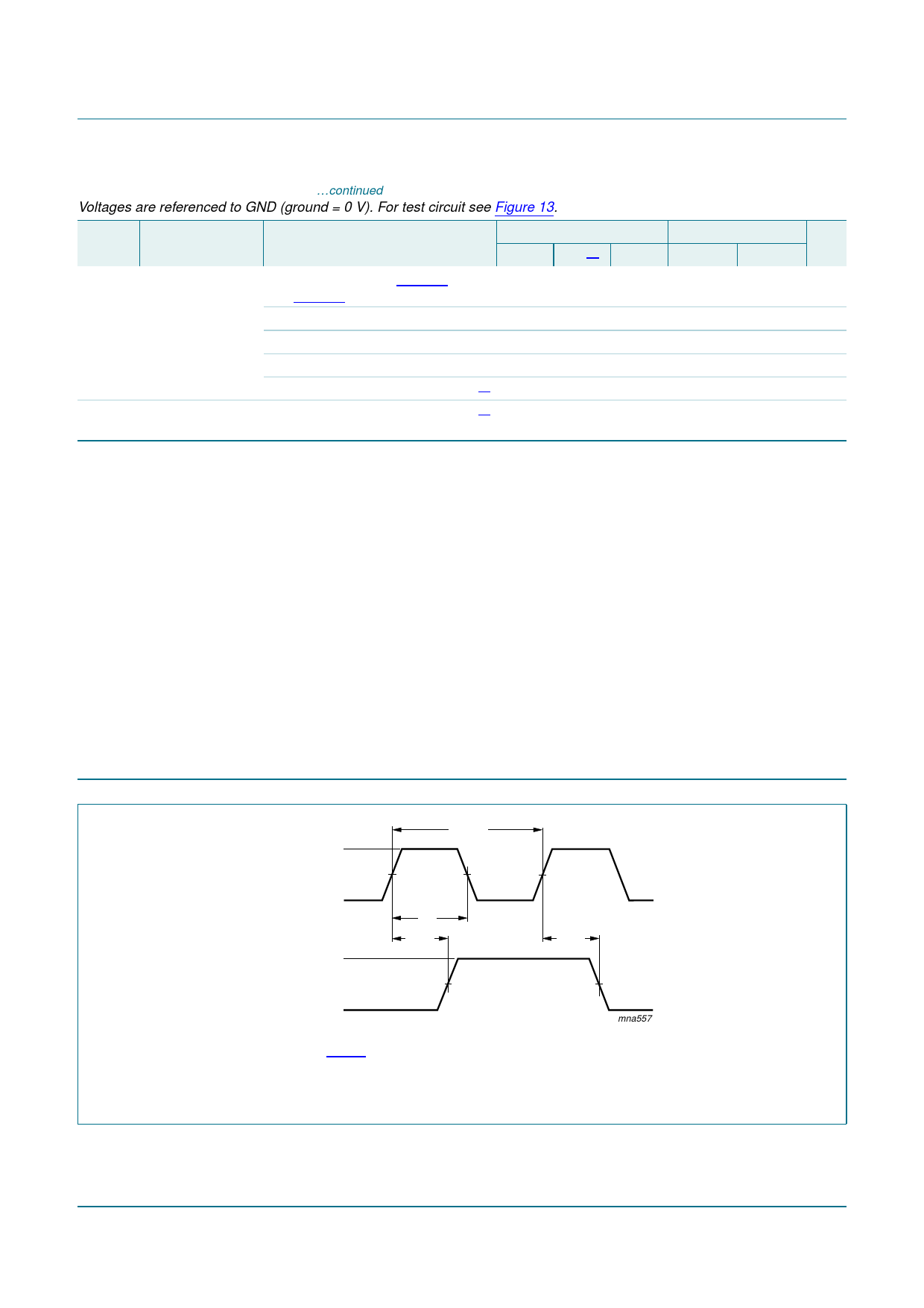
12. Waveforms
9,
6+&3LQSXW
*1'
92+
4 6RXWSXW
92/
IPD[
90
W:
W 3/+
90
W 3+/
PQD
Fig 8.
Measurement points are given in Table 8.
VOL and VOH are typical output voltage drops that occur with the output load.
The shift clock (SHCP) to serial data output (Q7S) propagation delays, the shift clock pulse width and
maximum shift clock frequency
74LV595
Product data sheet
All information provided in this document is subject to legal disclaimers.
Rev. 4 — 18 March 2016
© Nexperia B.V. 2017. All rights reserved
10 of 20
Share Link: