P101W 데이터 시트보기 (PDF) - Vishay Semiconductors
부품명
상세내역
일치하는 목록
P101W Datasheet PDF : 6 Pages
| |||
P100 Series
Passivated Assembled Vishay High Power Products
Circuit Elements, 25 A
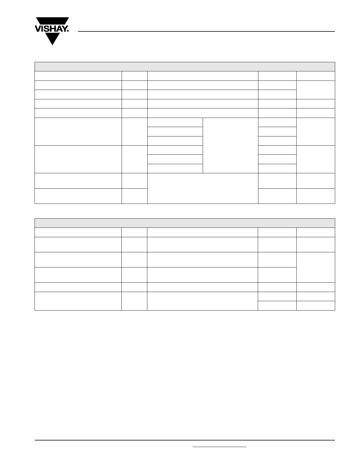
TRIGGERING
PARAMETER
Maximum peak gate power
Maximum average gate power
Maximum peak gate current
Maximum peak negative gate voltage
Maximum gate voltage
required to trigger
Maximum gate current
required to trigger
Maximum gate voltage
that will not trigger
Maximum gate current
that will not trigger
SYMBOL
PGM
PG(AV)
IGM
-VGM
VGT
IGT
VGD
IGD
TEST CONDITIONS
TJ = - 40 °C
TJ = 25 °C
TJ = 125 °C
TJ = - 40 °C
TJ = 25 °C
TJ = 125 °C
Anode supply =
6 V resistive load
TJ = 125 °C, rated VDRM applied
VALUES
8
2
2
10
3
2
1
90
60
35
0.2
2
UNITS
W
A
V
V
mA
V
mA
THERMAL AND MECHANICAL SPECIFICATIONS
PARAMETER
SYMBOL
TEST CONDITIONS
VALUES
UNITS
Maximum junction operating
and storage temperature range
TJ, TStg
- 40 to 125
°C
Maximum thermal resistance,
junction to case per junction
Maximum thermal resistance,
case to heatsink
RthJC
DC operation
RthCS Mounting surface, smooth and greased
2.24
K/W
0.10
Mounting torque, base to heatsink (1)
4
Nm
Approximate weight
58
g
2.0
oz.
Note
(1) A mounting compund is recommended and the torque should be checked after a period of 3 hours to allow for the spread of the compound
Document Number: 93754
Revision: 03-Jun-08
For technical questions, contact: ind-modules@vishay.com
www.vishay.com
3
Share Link: 