AD9831ASTZ 데이터 시트보기 (PDF) - Analog Devices
부품명
상세내역
일치하는 목록
AD9831ASTZ Datasheet PDF : 16 Pages
| |||
AD9831–SPECIFICATIONS1 (VDD = +3.3 V ؎ 10%; +5 V ؎ 10%; AGND = DGND = 0 V; TA = TMIN to TMAX; REFIN =
REFOUT; RSET = 3.9 k⍀; RLOAD = 300 ⍀ for IOUT unless otherwise noted)
Parameter
AD9831A
Units
Test Conditions/Comments
SIGNAL DAC SPECIFICATIONS
Resolution
10
Update Rate (fMAX)
25
IOUT Full Scale
4
5
Output Compliance
1.5
DC Accuracy
Integral Nonlinearity
±1
Differential Nonlinearity
± 0.5
DDS SPECIFICATIONS2
Dynamic Specifications
Signal to Noise Ratio
50
Total Harmonic Distortion
–53
Spurious Free Dynamic Range (SFDR)3
Narrow Band (± 50 kHz)
–72
–70
Wide Band (± 2 MHz)
–50
Clock Feedthrough
–60
Wake-Up Time4
1
Powerdown Option
Yes
Bits
MSPS nom
mA nom
mA max
V max
LSB typ
LSB typ
dB min
dBc max
dBc min
dBc min
dBc min
dBc typ
ms typ
fMCLK = 25 MHz, fOUT = 1 MHz
fMCLK = 25 MHz, fOUT = 1 MHz
fMCLK = 6.25 MHz, fOUT = 2.11 MHz
5 V Power Supply
3 V Power Supply
VOLTAGE REFERENCE
Internal Reference @ +25°C
TMIN to TMAX
REFIN Input Impedance
Reference TC
REFOUT Output Impedance
1.21
1.21 ± 7%
10
100
300
Volts typ
Volts min/max
MΩ typ
ppm/°C typ
Ω typ
LOGIC INPUTS
VINH, Input High Voltage
VINL, Input Low Voltage
IINH, Input Current
CIN, Input Capacitance
POWER SUPPLIES
AVDD
DVDD
IAA
IDD
IAA + IDD5
Low Power Sleep Mode6
VDD – 0.9
0.9
10
10
V min
V max
µA max
pF max
2.97/5.5
2.97/5.5
12
2.5 + 0.33/MHz
15
24
1
V min/V max
V min/V max
mA max
mA typ
mA max
mA max
mA max
5 V Power Supply
5 V Power Supply
3 V Power Supply
5 V Power Supply
1 MΩ Resistor Tied Between REFOUT and AGND
NOTES
1Operating temperature range is as follows: A Version: –40°C to +85°C.
2100% production tested.
3fMCLK = 6.25 MHz, Frequency Word = 5671C71C HEX, fOUT = 2.11 MHz.
4See Figure 11. To reduce the wake-up time at low power supplies and low temperature, the use of an external reference is suggested.
5Measured with the digital inputs static and equal to 0 V or DVDD.
6The Low Power Sleep Mode current is typically 2 mA when a 1 MΩ resistor is not tied between REFOUT and AGND.
The AD9831 is tested with a capacitive load of 50 pF. The part can be operated with higher capacitive loads, but the magnitude of the analog output will be attenu-
ated. For example, a 5 MHz output signal will be attenuated by 3 dB when the load capacitance equals 85 pF.
Specifications subject to change without notice.
10nF
RSET
3.9kΩ
REFOUT
ON-BOARD
REFERENCE
REFIN FS
ADJUST
FULL-SCALE
CONTROL
COMP
AVDD
10nF
12
SIN
ROM
10-BIT DAC
AD9831
IOUT
300Ω
50pF
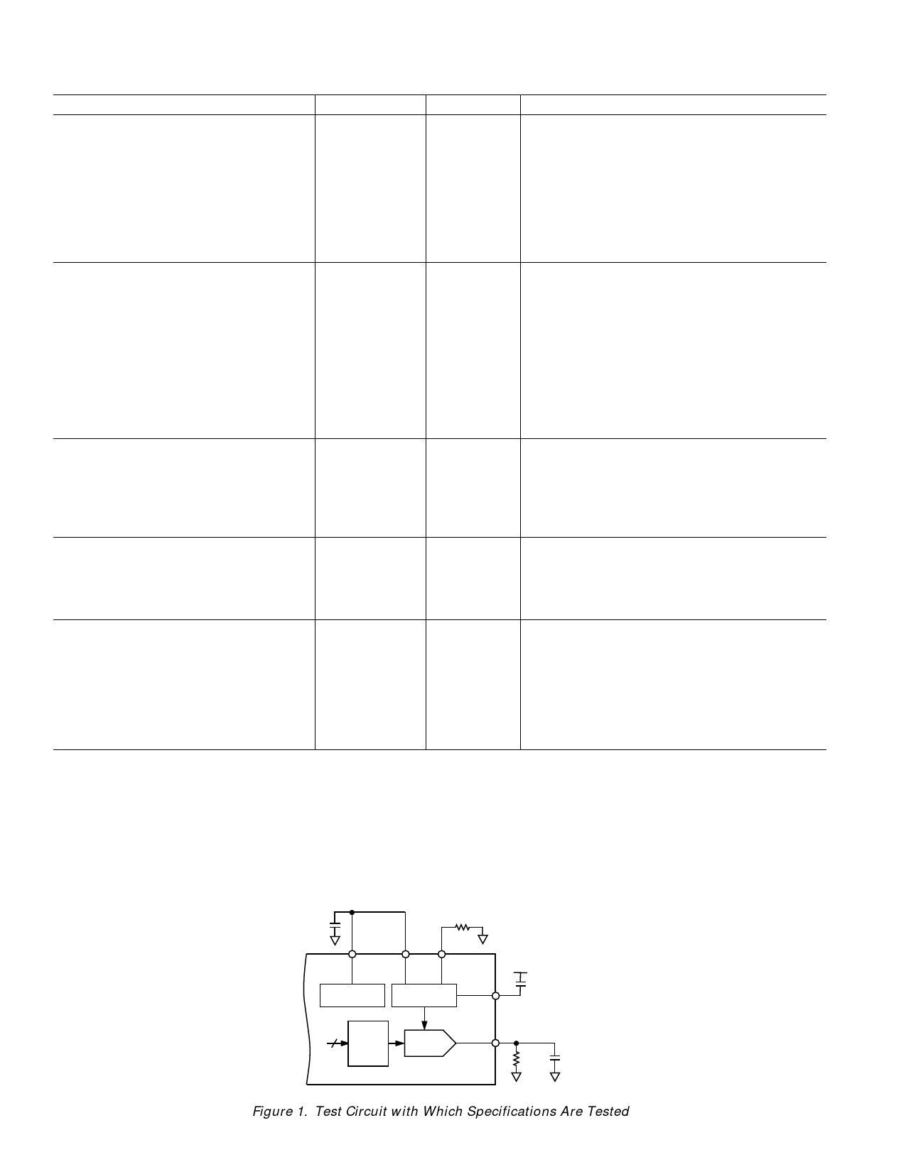
Figure 1. Test Circuit with Which Specifications Are Tested
–2–
REV. B
Share Link: 