74HC367D 데이터 시트보기 (PDF) - NXP Semiconductors.
부품명
상세내역
일치하는 목록
74HC367D Datasheet PDF : 18 Pages
| |||
Nexperia
74HC367; 74HCT367
Hex buffer/line driver; 3-state
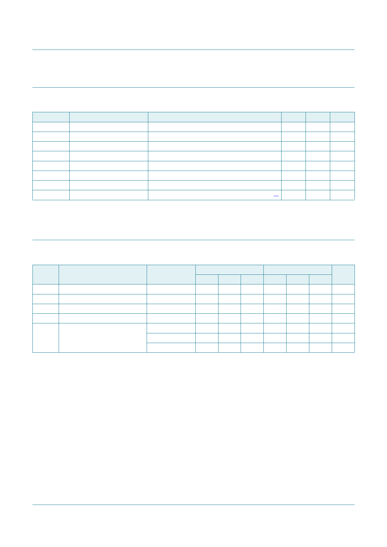
7. Limiting values
Table 4. Limiting values
In accordance with the Absolute Maximum Rating System (IEC 60134). Voltages are referenced to GND (ground = 0 V).
Symbol
Parameter
Conditions
Min Max Unit
VCC
supply voltage
IIK
input clamping current
VI < 0.5 V or VI > VCC + 0.5 V
IOK
output clamping current
VO < 0.5 V or VO > VCC + 0.5 V
IO
output current
0.5 V < VO < VCC + 0.5 V
0.5
+7 V
-
20 mA
-
20 mA
-
35 mA
ICC
IGND
Tstg
Ptot
supply current
ground current
storage temperature
total power dissipation
SO16, SSOP16 and TSSOP16 packages
-
70
65
[1]
-
70 mA
- mA
+150 C
500 mW
[1] For SO16 packages: Ptot derates linearly with 8 mW/K above 70 C.
For SSOP16 and TSSOP16 packages: Ptot derates linearly with 5.5 mW/K above 60 C.
8. Recommended operating conditions
Table 5. Recommended operating conditions
Voltages are referenced to GND (ground = 0 V)
Symbol Parameter
Conditions
VCC
VI
VO
Tamb
t/V
supply voltage
input voltage
output voltage
ambient temperature
input transition rise and fall rate
VCC = 2.0 V
VCC = 4.5 V
VCC = 6.0 V
74HC367
Min Typ Max
2.0 5.0 6.0
0
-
VCC
0
-
VCC
40 +25 +125
-
-
625
-
1.67 139
-
-
83
74HCT367
Min Typ Max
4.5 5.0 5.5
0
-
VCC
0
-
VCC
40 +25 +125
-
-
-
-
1.67 139
-
-
-
Unit
V
V
V
C
ns/V
ns/V
ns/V
74HC_HCT367
Product data sheet
All information provided in this document is subject to legal disclaimers.
Rev. 3 — 17 October 2016
© Nexperia B.V. 2017. All rights reserved
5 of 18
Share Link: 