74ABT827 데이터 시트보기 (PDF) - NXP Semiconductors.
부품명
상세내역
일치하는 목록
74ABT827 Datasheet PDF : 14 Pages
| |||
NXP Semiconductors
74ABT827
10-bit buffer/line driver; non-inverting; 3-state
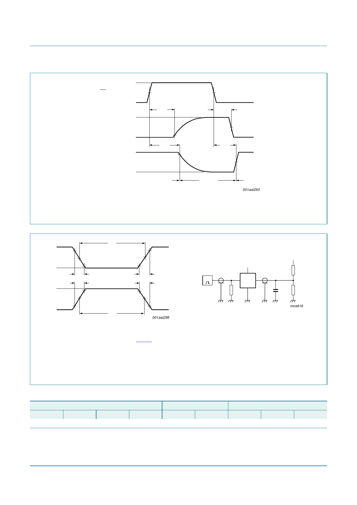
VI
OEn input
GND
3.5 V
output
LOW-to-OFF
OFF-to-LOW
VOL
output
VOH
HIGH-to-OFF
OFF-to-HIGH
GND
VM
tPLZ
tPZL
tPHZ
VOL + 0.3 V
VOH − 0.3 V
VM
tPZH
VM
outputs
enabled
outputs
disabled
outputs
enabled
001aal293
Fig 6.
VM = 1.5 V
VOL and VOH are typical voltage output levels that occur with the output load.
3-state enable and disable times
VI
negative
pulse
0V
VI
positive
pulse
0V
90 %
10 %
VM
10 %
tf
tr
90 %
VM
tW
90 %
VM
10 %
tr
tf
90 %
VM
10 %
tW
001aai298
VI
G
VCC
VO
DUT
RT
a. Input pulse definition
b. Test circuit
Fig 7.
Test data and VEXT levels are given in Table 8.
RL = Load resistance.
CL = Load capacitance including jig and probe capacitance.
RT = Termination resistance should be equal to output impedance Zo of the pulse generator.
VEXT = Test voltage for switching times.
Test circuit for measuring switching times
VEXT
RL
CL
RL
mna616
Table 8.
Input
VI
3.0 V
Test data
fI
1 MHz
tW
500 ns
tr, tf
≤ 2.5 ns
Load
CL
50 pF
RL
500 Ω
VEXT
tPHL, tPLH
open
tPZH, tPHZ
open
tPZL, tPLZ
7.0 V
74ABT827_3
Product data sheet
All information provided in this document is subject to legal disclaimers.
Rev. 03 — 24 February 2010
© NXP B.V. 2010. All rights reserved.
7 of 14
Share Link: 