HEF4543B(2016) 데이터 시트보기 (PDF) - NXP Semiconductors.
부품명
상세내역
일치하는 목록
HEF4543B Datasheet PDF : 16 Pages
| |||
Nexperia
HEF4543B
BCD to 7-segment latch/decoder/driver
Table 7. Dynamic characteristics …continued
VSS = 0 V; Tamb = 25 C; For test circuit see Figure 7;unless otherwise specified.
Symbol Parameter
Conditions
VDD
Extrapolation formula[1]
th
hold time
Dn to LE;
see Figure 6
5V
10 V
15 V
tW
pulse width
pin LE HIGH;
minimum width;
see Figure 6
5V
10 V
15 V
Min Typ Max Unit
0 15 - ns
15
0
- ns
20
5
- ns
60 30
- ns
30 15
- ns
20 10
- ns
[1] The typical values of the propagation delay and transition times are calculated from the extrapolation formulas shown (CL in pF).
Table 8. Dynamic power dissipation PD
PD can be calculated from the formulas shown. VSS = 0 V; tr = tf 20 ns; Tamb = 25 C.
Symbol Parameter
VDD
Typical formula for PD (W)
where:
PD
dynamic power 5 V
PD = 2200 fi + (fo CL) VDD2
fi = input frequency in MHz,
dissipation
10 V
PD = 10400 fi + (fo CL) VDD2
fo = output frequency in MHz,
15 V
PD = 33000 fi + (fo CL) VDD2
CL = output load capacitance in pF,
VDD = supply voltage in V,
(CL fo) = sum of the outputs.
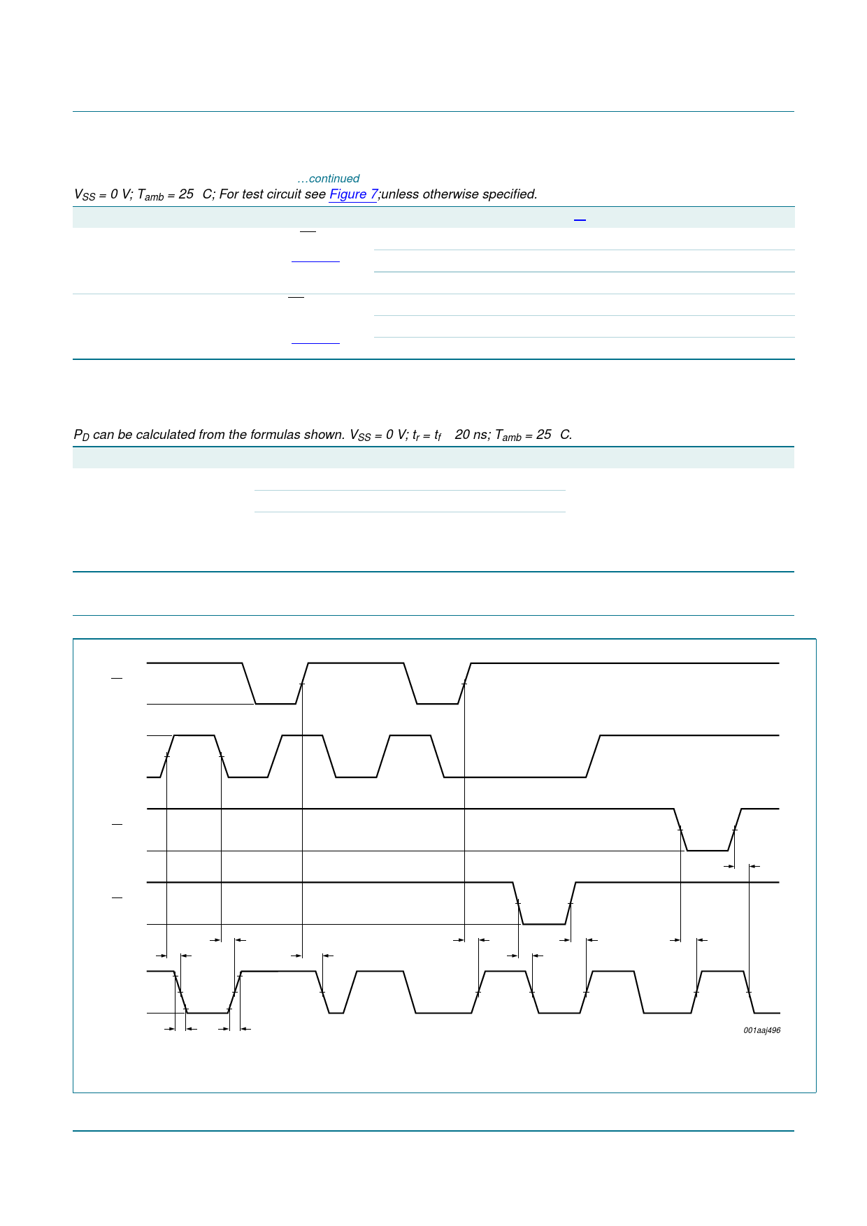
11. Waveforms
9,
/(
966
90
90
9,
'
90
966
9,
%/
966
92+
4J
92/
W7+/
W3+/
90
W3/+
W7/+
W3+/
Conditions: D3 = LOW and D0 = D1 = HIGH.
Fig 5. Propagation delays and output transitions times
90
W3/+
W3+/
W3/+
DDM
HEF4543B
Product data sheet
All information provided in this document is subject to legal disclaimers.
Rev. 7 — 1 April 2016
© Nexperia B.V. 2017. All rights reserved
8 of 16
Share Link: 