74HC4511 데이터 시트보기 (PDF) - NXP Semiconductors.
부품명
상세내역
일치하는 목록
74HC4511 Datasheet PDF : 18 Pages
| |||
Nexperia
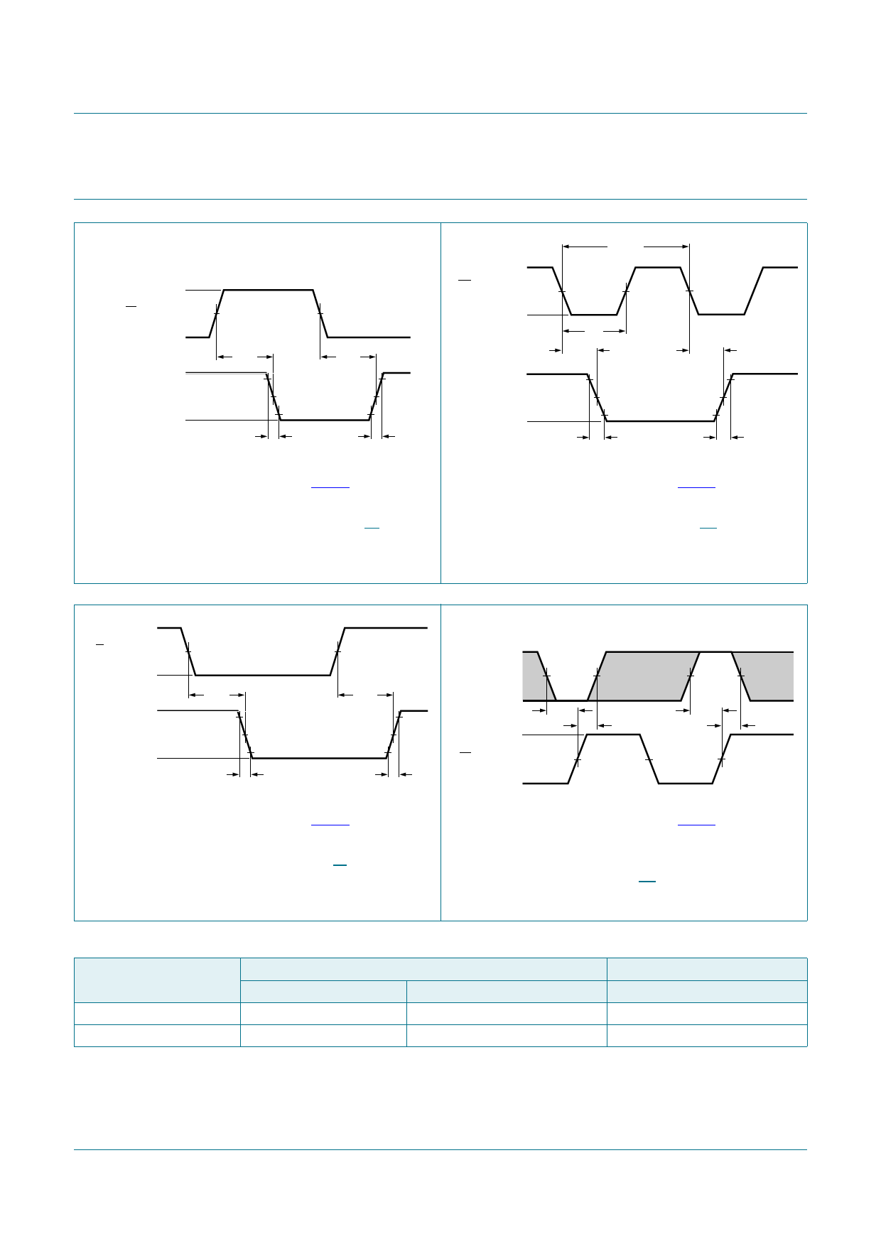
11. Waveforms
74HC4511; 74HCT4511
BCD to 7-segment latch/decoder/driver
9,
$'/7LQSXW
*1'
92+
DJRXWSXW
92/
90
W3+/
90
W7+/
W3/+
W7/+
DDD
9,
/(LQSXW
*1'
92+
DJRXWSXW
92/
IPD[
90
W:
W3+/
90
W7+/
W3/+
W7/+
DDD
Fig 8.
Measurement points are given in Table 8.
Logic levels VOL and VOH are typical output voltage
levels that occur with the output load.
Waveforms showing the input (A-D, LT) to
output (a-g) propagation delays and the output
transition times
Fig 9.
Measurement points are given in Table 8.
Logic levels VOL and VOH are typical output voltage
levels that occur with the output load.
Waveforms showing the input (LE) to output
(a-g) propagation delays; the latch enable
pulse width and the output transition times
9,
%,LQSXW
*1'
92+
DJRXWSXW
92/
90
W3+/
90
W7+/
W3/+
W7/+
DDD
9,
$'LQSXW
*1'
9,
/(LQSXW
*1'
90
WVX
WK
90
WVX
WK
DDD
Measurement points are given in Table 8.
Logic levels VOL and VOH are typical output voltage
levels that occur with the output load.
Fig 10. Waveforms showing the input (BI) to output
(a-g) propagation delays and the output
transition times
Measurement points are given in Table 8.
The shaded areas indicate when the input is permitted to
change for predictable output performance.
Fig 11. Waveforms showing the data set-up and hold
times for a-g input to LE input
Table 8. Measurement points
Type
Input
74HC4511
74HCT4511
VM
0.5 VCC
1.3 V
VI
GND to VCC
GND to 3 V
Output
VM
0.5 VCC
1.3 V
74HC_HCT4511
Product data sheet
All information provided in this document is subject to legal disclaimers.
Rev. 3 — 15 November 2016
© Nexperia B.V. 2017. All rights reserved
11 of 18
Share Link: 