SCY99079CDR2G 데이터 시트보기 (PDF) - ON Semiconductor
부품명
상세내역
일치하는 목록
SCY99079CDR2G Datasheet PDF : 28 Pages
| |||
DAP018A/B/C/D/F
RoppU
Rbias
This point will
be adjusted to
reduce the ref
at hi line to the
desired level.
Iopp
RoppL
OPP
Dz
VCC aux
+
Swings to:
N1Vout during toff
−N2Vout during ton
VDD
from FB
K1 SUM2
ref
K2
0.8 V ±5%
ref = 0.8 V + VOPP
(VOPP is negative)
Reset
-
+
CS
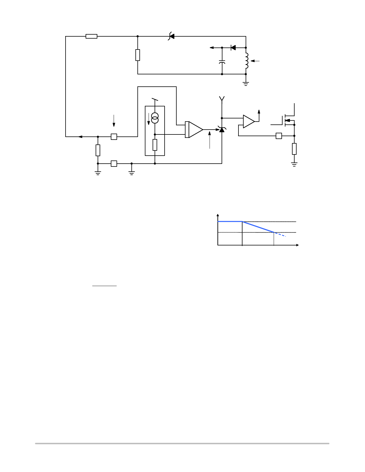
Figure 54. The Zener Diode can Introduce a Threshold which
Disables OPP at Low Line for Maximum Power Capability
Suppose we need a threshold placed at 150 Vdc. In that
case, give the turn ratio, we need to install a zener diode
featuring the following breakdown voltage:
Vz + 150 0.16 + 24 V
(eq. 8)
In high line conditions (Vbulk = 375 Vdc), the voltage on the
zener diode voltage will now swing to:
(eq. 9)
Vaux + −N2Vin,max ) 24 + −0.16 375 ) 24 + −36 V
Applying Equation 6 again, we have:
ROPPU
+
36 * 0.16
0.16ń1 k
+
224
kW
(eq. 10)
The new compensation now looks like what Figure 55
shows:
Peak current
setpoint
100%
20%
150
375
Vbulk
Figure 55. The Addition of the Zener Diode
Introduces a Threshold at 150 Vdc
The bias resistor Rbias, makes sure that enough current
circulates in the zener diode to make it work far enough from
its knee. The tradeoff includes the power consumption
brought by the addition of this new component. Further
reduction can be obtained by inserting a standard diode in
series with the zener to block the positive excursion.
http://onsemi.com
27
Share Link: 