TDF1747 데이터 시트보기 (PDF) - STMicroelectronics
부품명
상세내역
일치하는 목록
TDF1747 Datasheet PDF : 11 Pages
| |||
TDE1747 - TDF1747
ELECTRICAL CHARACTERISTICS Tj = – 25 to +85 °C, VCC = 8 to 45 V, unless otherwise specified
(note 1).
Symbol
VIO
IIB
ICC
Parameter
Input Offset Voltage - (note 2)
Input Bias Current
Supply Current (VCC = + 24 V, IO = 0)
High Level
Low Level
Min. Typ. Max. Unit
–
2
50
mV
–
0.1
1.5
mA
–
4
6
mA
–
2
4
mA
VI(max)
Common-mode Input Voltage Range
2
–
VCC–2
V
ISC
Short-circuit Current Limit
t(s) (Tamb = + 25 °C, VCC = + 24)
RSC = 1.5 Ω
RSC = ∞
TDE1747 –
–
480
–
mA
35
50
mA
roduc VCC–VO
Output Saturation Voltage (output high)
(RSC = 0, VI+–VI– ≥ 50 mV)
IO = 300 mA, Tj = + 25 °C
Tj = + 150 °C
–
1.15 1.4
V
–
1.05 1.3
V
P IOL
Low Level Output Current
te (VO = 0, VCC = + 24 V)
le Tj = + 25 °C
–
0.01 10
µA
o Notes :
bs 1) For operating at high temperature, the TDE/TDF1747, must be derated based on a + 150 C maximum junction temperature and a
junction-ambient thermal resistance of 120 °C/W for Minidip and 100 °C/W for the SO14.
- O 2) The offset voltage given is the maximum value of input voltage required to drive the output voltage within 2 V of the ground or the supply
voltage.
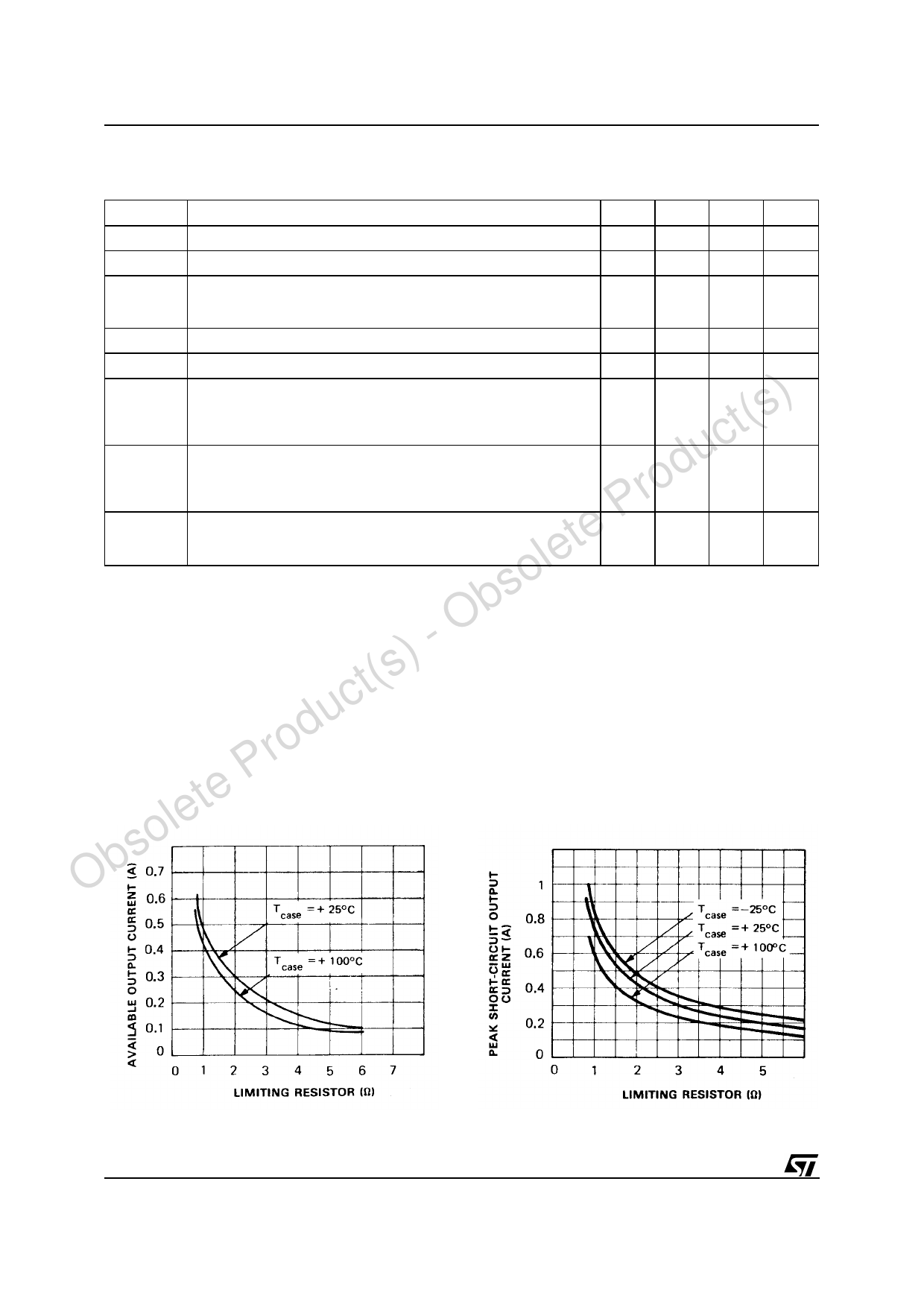
te Product(s) Figure 1: Available Output Current vs. Limiting
ObsoleResistor
Figure 2: Peak Short-circuit Output Current vs.
Limiting Resistor
4/11
Share Link: 