NTE1901 데이터 시트보기 (PDF) - NTE Electronics
부품명
상세내역
일치하는 목록
NTE1901
NTE Electronics

NTE1901 Datasheet PDF : 3 Pages
| |||
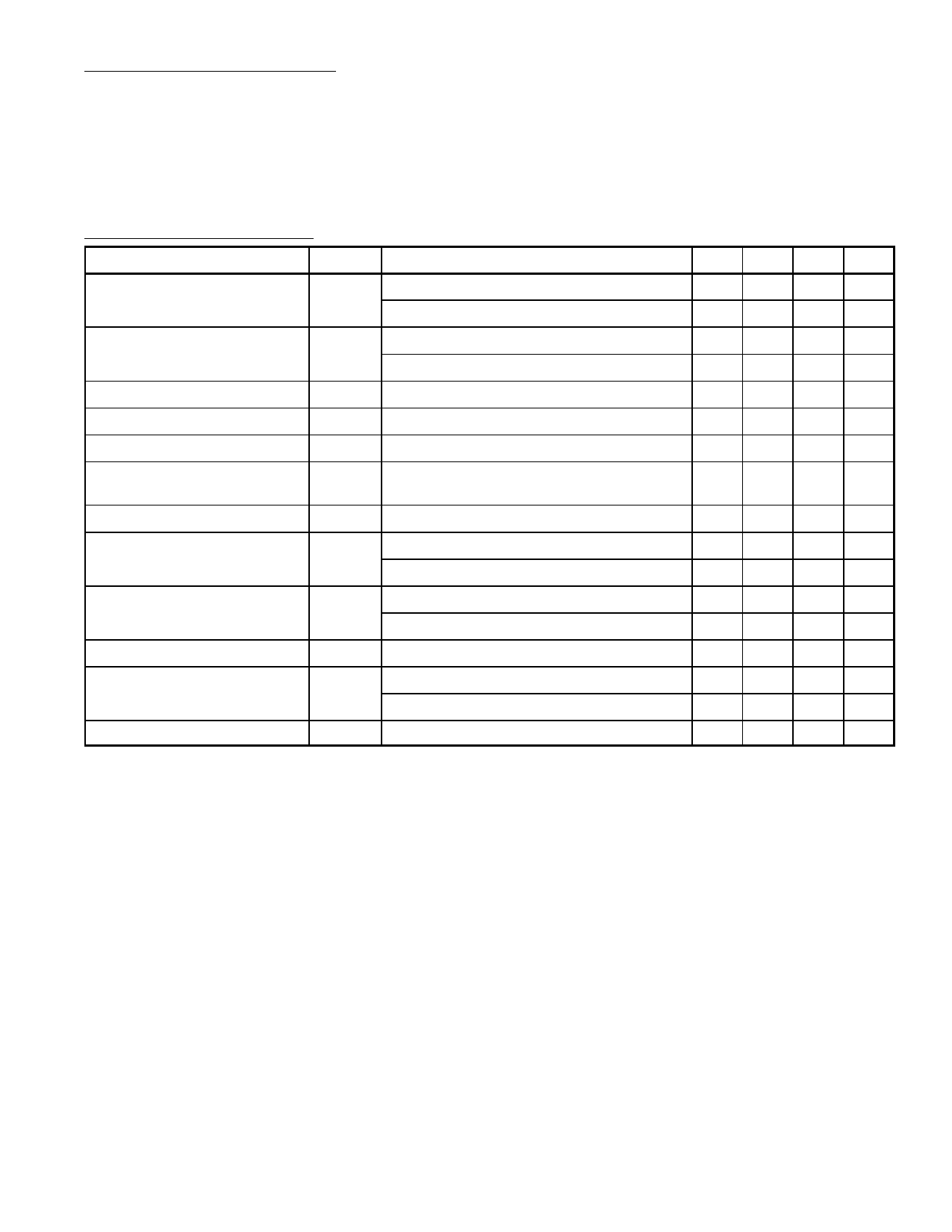
Absolute Maximum Ratings: (TA = +25°C unless otherwise specified)
Power Dissipation, PD . . . . . . . . . . . . . . . . . . . . . . . . . . . . . . . . . . . . . . . . . . . . . . . . . . Internally Limited
Input–Output Voltage Differential, VI – VO . . . . . . . . . . . . . . . . . . . . . . . . . . . . . . . . . . . . . . . . . . . . . 40V
Operating Junction Temperature Range, TJ . . . . . . . . . . . . . . . . . . . . . . . . . . . . . . . . . . –40° to +125°C
Storage Temperature Range, Tstg . . . . . . . . . . . . . . . . . . . . . . . . . . . . . . . . . . . . . . . . . . –55° to +150°C
Lead Temperature (During Soldering, 10sec), TL . . . . . . . . . . . . . . . . . . . . . . . . . . . . . . . . . . . . +300°C
Electrical Characteristics: (Note 1 unless otherwise specified)
Parameter
Symbol
Test Conditions
Min Typ Max Unit
Line Regulation
RegLine TA = +25°C, 3V ≤ (VIN – VO) ≤ 40V, Note 2 – 0.01 0.04 %/V
3V ≤ (VIN – VO) ≤ 40V, Note 2
– 0.02 0.07 %/V
Load Regulation
Thermal Regulation
RegLoad
TA = +25°C, 5mA ≤ IO ≤ 100mA, Note 2
5mA ≤ IO ≤ 100mA, Note 2
TA = +25°C, 10ms Pulse
– 0.1 0.5 %
– 0.1 0.5 %
– 0.04 0.2 %/W
Adjustment Pin Current
IAdj
– 50 100 µA
Adjustment Pin Current Change
Reference Voltage
IAdj 5mA ≤ IL ≤ 100mA, 3V ≤ (VIN – VO) ≤ 40V
–
0.2 5.0 µA
Vref 5mA ≤ IL ≤ 100mA, 3V ≤ (VIN – VO) ≤ 40V, 1.20 1.25 1.30 V
P ≤ 625mW, Note 3
Temperature Stability
TS –25°C ≤ TJ ≤ +125°C
– 0.65 – %
Minimum Load Currnt
MaximumOutput Current Limit
IL(min)
Imax
(VIN – VO) ≤ 40V
3V ≤ (VIN – VO) ≤ 15V
3V ≤ (VIN – VO) ≤ 13V
– 3.5 5.0 mA
– 2.2 3.5 mA
100 200 300 mA
(VIN – VO) ≤ 40V
25 50 150 mA
RMS Output Noise, % of VOUT N TA = +25°C, 10Hz ≤ f ≤ +10kHz
– 0.003 – %
Ripple Rejection Ratio
Long Term Stability
RR VOUT = –10V, f = 120Hz, CADJ = 0
CADJ = 10µF
S TJ = +125°C, 100 Hours
– 65 – dB
66 80 – dB
– 0.3 1.0 %
Note 1. Unless otherwise noted, these specifications apply: –25° ≤ TJ ≤ +125°C, VIN – VOUT = 5V,
IOUT = 40mA, and IMAX = 100mA. Although power dissipation is internally limited, these
specifications are applicable for power dissipations up to 625mW.
Note 2. Regulation is measured at constant junction temperature, using pulse testing with low duty
cycle. Changes in output voltage due to heating effects are covered under the specifications
for thermal regulation.
Note 3. Thermal resistance o the TO92 package is 180°C/W junction to ambient with 0.4” leads from
a PC board and 160°C/W junction to ambient with 0.125” lead length to PC board.
Share Link: