IRG4BC10S 데이터 시트보기 (PDF) - International Rectifier
부품명
상세내역
일치하는 목록
IRG4BC10S Datasheet PDF : 8 Pages
| |||
IRG4BC10S
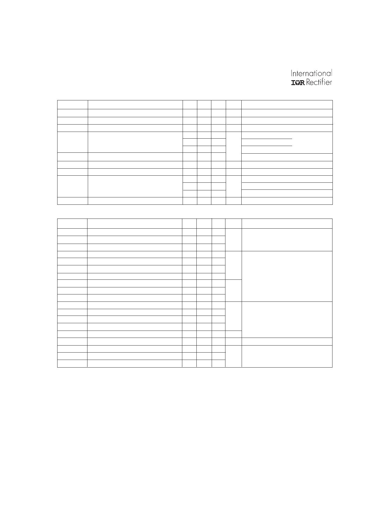
Electrical Characteristics @ TJ = 25°C (unless otherwise specified)
V(BR)CES
V(BR)ECS
∆V(BR)CES/∆TJ
VCE(ON)
VGE(th)
∆VGE(th)/∆TJ
gfe
ICES
IGES
Parameter
Collector-to-Emitter Breakdown Voltage
Emitter-to-Collector Breakdown Voltage T
Temperature Coeff. of Breakdown Voltage
Collector-to-Emitter Saturation Voltage
Gate Threshold Voltage
Temperature Coeff. of Threshold Voltage
Forward Transconductance U
Zero Gate Voltage Collector Current
Gate-to-Emitter Leakage Current
Min. Typ. Max. Units
Conditions
600 — — V VGE = 0V, IC = 250µA
18 — — V VGE = 0V, IC = 1.0A
— 0.64 — V/°C VGE = 0V, IC = 1.0mA
— 1.58 1.7
IC = 8.0A
VGE = 15V
— 2.05 —
V
IC = 14A
See Fig.2, 5
— 1.68 —
IC = 8.0A , TJ = 150°C
3.0 — 6.0
VCE = VGE, IC = 250µA
— -9.5 — mV/°C VCE = VGE, IC = 250µA
3.7 5.5 — S VCE = 100V, IC = 8.0A
— — 250 µA VGE = 0V, VCE = 600V
— — 2.0
VGE = 0V, VCE = 10V, TJ = 25°C
— — 1000
VGE = 0V, VCE = 600V, TJ = 150°C
— — ±100 nA VGE = ±20V
Switching Characteristics @ TJ = 25°C (unless otherwise specified)
Qg
Qge
Qgc
td(on)
tr
td(off)
tf
Eon
Eoff
Ets
td(on)
tr
td(off)
tf
Ets
LE
Cies
Coes
Cres
Notes:
Parameter
Total Gate Charge (turn-on)
Gate - Emitter Charge (turn-on)
Gate - Collector Charge (turn-on)
Turn-On Delay Time
Rise Time
Turn-Off Delay Time
Fall Time
Turn-On Switching Loss
Turn-Off Switching Loss
Total Switching Loss
Turn-On Delay Time
Rise Time
Turn-Off Delay Time
Fall Time
Total Switching Loss
Internal Emitter Inductance
Input Capacitance
Output Capacitance
Reverse Transfer Capacitance
Min.
—
—
—
—
—
—
—
—
—
—
—
—
—
—
—
—
—
—
—
Typ. Max.
15 22
2.4 3.6
6.5 9.8
25 —
28 —
630 950
710 1100
0.14 —
2.58 —
2.72 4.3
24 —
31 —
810 —
1300 —
3.94 —
7.5 —
280 —
30 —
4.0 —
Units
nC
ns
mJ
ns
mJ
nH
pF
Conditions
IC = 8.0A
VCC = 400V
See Fig. 8
VGE = 15V
TJ = 25°C
IC = 8.0A, VCC = 480V
VGE = 15V, RG = 100Ω
Energy losses include "tail"
See Fig. 9, 10, 14
TJ = 150°C,
IC = 8.0A, VCC = 480V
VGE = 15V, RG = 100Ω
Energy losses include "tail"
See Fig. 11, 14
Measured 5mm from package
VGE = 0V
VCC = 30V
See Fig. 7
ƒ = 1.0MHz
Q Repetitive rating; VGE = 20V, pulse width limited by
max. junction temperature. ( See fig. 13b )
T Pulse width ≤ 80µs; duty factor ≤ 0.1%.
R VCC = 80%(VCES), VGE = 20V, L = 10µH, RG = 100Ω,
(See fig. 13a)
U Pulse width 5.0µs, single shot.
S Repetitive rating; pulse width limited by maximum
junction temperature.
2
www.irf.com
Share Link: 