74HC4852D-Q100 데이터 시트보기 (PDF) - Nexperia B.V. All rights reserved
부품명
상세내역
일치하는 목록
74HC4852D-Q100
Nexperia B.V. All rights reserved

74HC4852D-Q100 Datasheet PDF : 21 Pages
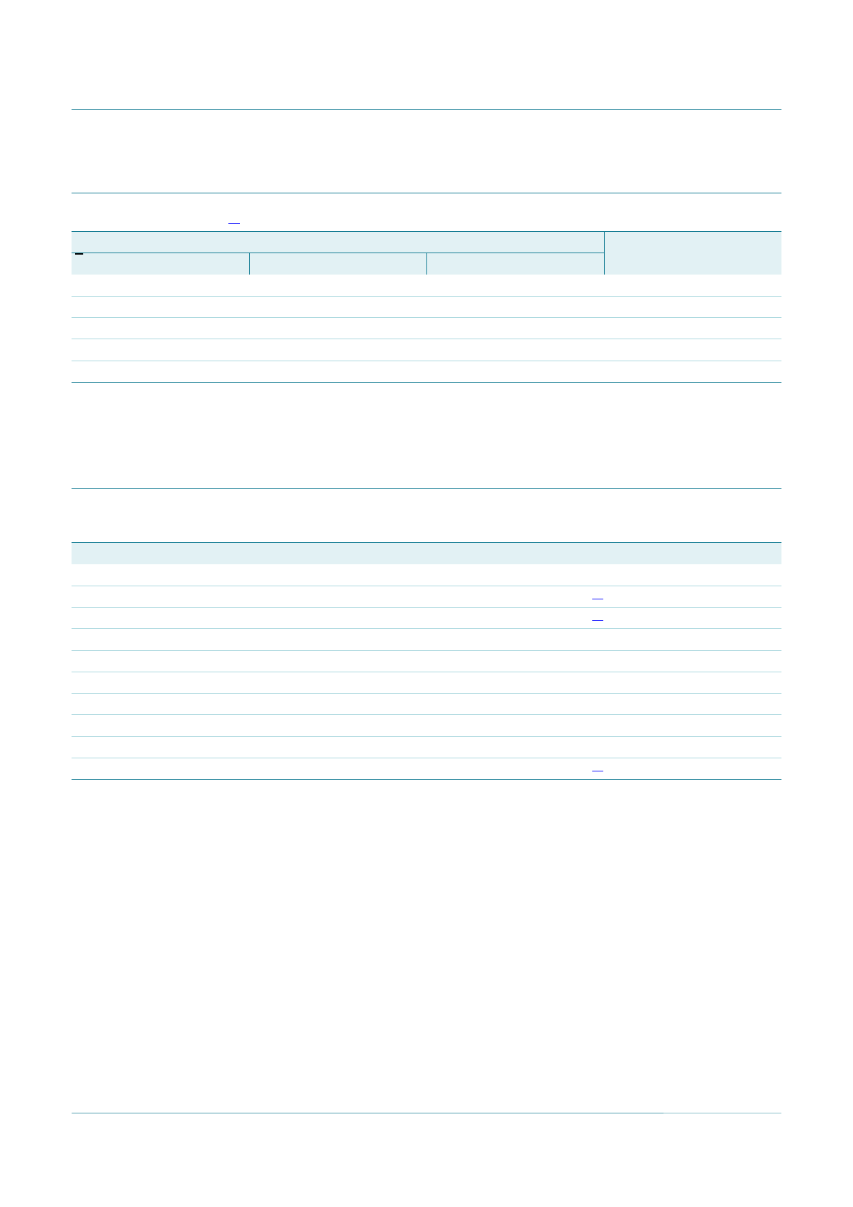
| |||
Nexperia
74HC4852-Q100; 74HCT4852-Q100
Dual 4-channel analog multiplexer/demultiplexer with injection-current
effect control
7. Functional description
Table 3. Function table[1]
Input
Channel ON
E
S1
S0
L
L
L
nY0 to nZ
L
L
H
nY1 to nZ
L
H
L
nY2 to nZ
L
H
H
nY3 to nZ
H
X
X
-
[1] H = HIGH voltage level;
L = LOW voltage level;
X = don’t care.
8. Limiting values
Table 4. Limiting values
In accordance with the Absolute Maximum Rating System (IEC 60134). Voltages are referenced to GND (ground = 0 V).
Symbol
Parameter
Conditions
Min Max
Unit
VCC
VI
VSW
IIK
ISK
ISW
ICC
IGND
Tstg
Ptot
supply voltage
input voltage
switch voltage
input clamping current
switch clamping current
switch current
supply current
ground current
storage temperature
total power dissipation
0.5 +7.0
V
[1] 0.5 VCC + 0.5 V
[2] 0.5 VCC + 0.5 V
VI < 0.5 V or VI > VCC + 0.5 V
-
20
mA
VSW < 0.5 V or VSW > VCC + 0.5 V
-
20
mA
VSW > 0.5 V or VSW < VCC + 0.5 V
-
25
mA
-
50
mA
50 -
mA
65 +150
C
Tamb = 40 C to +125 C
[3] -
500
mW
[1] The minimum and maximum input voltage rating may be exceeded if the input clamping current rating is observed.
[2] The minimum and maximum switch voltage rating may be exceeded if the switch clamping current rating is observed.
[3] For SO16 package: Ptot derates linearly with 8 mW/K above 70 C.
For TSSOP16 package: Ptot derates linearly with 5.5 mW/K above 60 C.
For DHVQFN16 packages: Ptot derates linearly with 4.5 mW/K above 60 C.
74HC_HCT4852_Q100
Product data sheet
All information provided in this document is subject to legal disclaimers.
Rev. 1 — 12 July 2012
© Nexperia B.V. 2017. All rights reserved
5 of 21
Share Link: