LT1617 데이터 시트보기 (PDF) - Linear Technology
부품명
상세내역
일치하는 목록
LT1617 Datasheet PDF : 8 Pages
| |||
LT1617/LT1617-1
APPLICATIO S I FOR ATIO
Choosing an Inductor
Several recommended inductors that work well with the
LT1617 and LT1617-1 are listed in Table 1, although there
are many other manufacturers and devices that can be
used. Consult each manufacturer for more detailed infor-
mation and for their entire selection of related parts. Many
different sizes and shapes are available. Use the equations
and recommendations in the next few sections to find the
correct inductance value for your design.
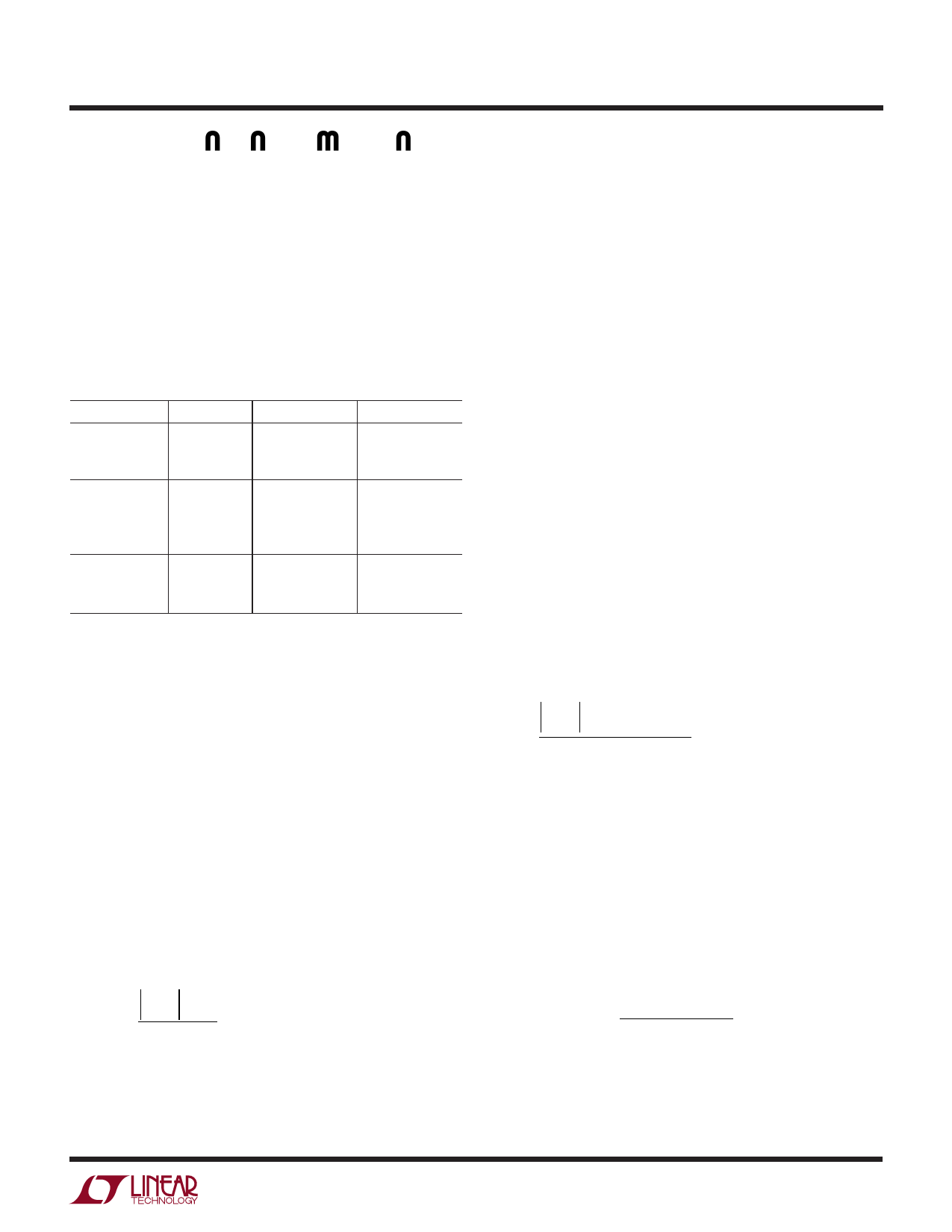
Table 1. Recommended Inductors
PART
VALUE (µH) MAX DCR (Ω)
LQH3C4R7
4.7
0.26
LQH3C100
10
0.30
LQH3C220
22
0.92
CD43-4R7
4.7
0.11
CD43-100
10
0.18
CDRH4D18-4R7
4.7
0.16
CDRH4D18-100
10
0.20
DO1608-472
4.7
0.09
DO1608-103
10
0.16
D01608-223
22
VENDOR
Murata
(714) 852-2001
www.murata.com
Sumida
(847) 956-0666
www.sumida.com
Coilcraft
(847) 639-6400
www.coilcraft.com
Inductor Selection—Inverting Regulator
The formula below calculates the appropriate inductor
value to be used for an inverting regulator using the
LT1617 or LT1617-1 (or at least provides a good starting
point). This value provides a good tradeoff in inductor size
and system performance. Pick a standard inductor close
to this value (both inductors should be the same value). A
larger value can be used to slightly increase the available
output current, but limit it to around twice the value
calculated below, as too large of an inductance will in-
crease the output voltage ripple without providing much
additional output current. A smaller value can be used
(especially for systems with output voltages greater than
12V) to give a smaller physical size. Inductance can be
calculated as:
For higher output voltages, the formula above will give
large inductance values. For a 2V to 20V converter (typical
LCD bias application), a 47µH inductor is called for with
the above equation, but a 10µH or 22µH inductor could be
used without excessive reduction in maximum output
current.
Inductor Selection—Inverting Charge Pump Regulator
For the inverting regulator, the voltage seen by the internal
power switch is equal to the sum of the absolute value of
the input and output voltages, so that generating high
output voltages from a high input voltage source will often
exceed the 36V maximum switch rating. For instance, a
12V to – 30V converter using the inverting topology would
generate 42V on the SW pin, exceeding its maximum
rating. For such a system, an inverting charge pump is the
best topology.
The formula below calculates the approximate inductor
value to be used for an inverting charge pump regulator
using the LT1617. As for the boost inductor selection, a
larger or smaller value can be used. For designs with
varying VIN such as battery powered applications, use the
minimum VIN value in the equation below.
( ) VOUT − VIN MIN + VD
L=
ILIM
tOFF
Current Limit Overshoot
For the constant off-time control scheme of the LT1617,
the power switch is turned off only after the 350mA (or
100mA) current limit is reached. There is a 100ns delay
between the time when the current limit is reached and
when the switch actually turns off. During this delay, the
inductor current exceeds the current limit by a small
amount. The peak inductor current can be calculated by:
VOUT + VD
L = 2 ILIM
tOFF
where VD = 0.4V (Schottky diode voltage), ILIM = 350mA or
100mA, and tOFF = 400ns.
IPEAK
=
ILIM
+
VIN(MAX)
L
−
VSAT
100ns
Where VSAT = 0.25V (switch saturation voltage). The
current overshoot will be most evident for systems with
high input voltages and for systems where smaller induc-
5
Share Link: 