T7237 데이터 시트보기 (PDF) - Agere -> LSI Corporation
부품명
상세내역
일치하는 목록
T7237 Datasheet PDF : 116 Pages
| |||
T7256 Single-Chip NT1 (SCNT1) Transceiver
Data Sheet
January 1998
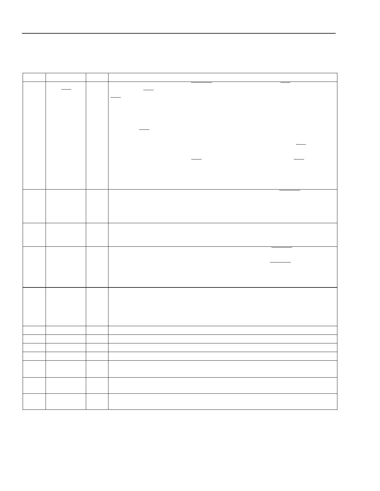
Pin Information (continued)
Table 1. Pin Descriptions (continued)
Pin Symbol Type*
Name/Function
11 ACTMODE/ Iu/O ACT Bit Mode. Upon exiting RESET, the state of ACTMODE/INT is read and if
INT
ACTMODE/INT = 1 (default), bit ACTSEL = 1 (register GR2, bit 6). If ACTMODE/
INT= 0 (externally pulled down), then ACTSEL = 0. An internal 100 kΩ pull-up re-
sistor is on this pin.
Serial Interface Microprocessor Interrupt (Active-Low). Interrupt output for mi-
croprocessor. Any active, unmasked bit in interrupt registers UIR0, SIR0, or MIR0
will cause INT to go low. The bits in the interrupt registers UIR0, SIR0, and MIR0
will be set on a true condition, independent of the state of the corresponding mask
bits. If a masked, active interrupt bit is subsequently unmasked, the INT pin will go
low to indicate an interrupt for that condition. Reading UIR0, SIR0, or MIR0 clears
the entire register and forces INT high for 50 µs. After this interval, INT will again
reflect the state of any unmasked bit in these registers. The global interrupt register
(GIRO) provides a summary status of the UIR0, SIR0, and MIR0 interrupt registers
and indicates if one of the registers currently has an active, unmasked interrupt bit.
12 SYN8K_CTL Id SYN8K/LBIND Control. If this pin is low at the rising edge of RESET, the SYN8K/
/SDI
LBIND/FS pin performs the SYN8K function. Otherwise, the pin performs the LBIND
function. An internal 100 kΩ pull-down resistor is on this pin.
Serial Interface Data Input. Data input for microprocessor interface.
14
SDO
O Serial Interface Data Output. Data output for microprocessor interface. This pin is
3-stated at all times except for when a microprocessor read from the T7256 is taking
place.
15 AUTOACT/ Id Automatic Activation. If this pin is low at the rising edge of RESET, the AUTOACT
SCK
bit is written to 0, creating an activation attempt (see AUTOACT [register GR0, bit
6] description in Table 4). If pin is held high during external RESET, no activation is
attempted. An internal 100 kΩ pull-down resistor is on this pin.
Serial Interface Clock. Clock input for microprocessor interface.
17
CKOUT
O Clock Output. Clock output function to drive other board components. Powerup de-
fault state is high-impedance to minimize power consumption. Programmable via
microprocessor register (register GR0, bits 1 and 2) to provide 15.36 MHz output or
10.24 MHz output. If U-interface is active, the 10.24 MHz output is synchronous with
U-interface timing.
18
GNDO
— Crystal Oscillator Ground. Ground lead for crystal oscillator.
19
VDDO
— Crystal Oscillator Power. Power supply lead for crystal oscillator.
20
X1
O Crystal #1. Crystal connection #1 for 15.36 MHz oscillator.
21
22, 33,
39, 42
X2
VDDA
I Crystal #2. Crystal connection #2 for 15.36 MHz oscillator.
— Analog Power. 5 V ± 5% power supply leads for analog circuitry.
23
TNR
O Transmit Negative Rail for S/T-Interface. Negative output of S/T-interface analog
transmitter. Connect to transformer through a 121 Ω ± 1% resistor.
24
TPR
O Transmit Positive Rail for S/T-Interface. Positive output of S/T-interface analog
transmitter. Connect to transformer through a 121 Ω ± 1% resistor.
* Iu = input with internal pull-up; Id = input with internal pull-down.
8
Lucent Technologies Inc.
Share Link: 