NTE7126 데이터 시트보기 (PDF) - NTE Electronics
부품명
상세내역
일치하는 목록
NTE7126 Datasheet PDF : 3 Pages
| |||
Absolute Maximum Ratings (Cont’d): (TA = +25°C unless otherwise specified)
TR1 (Cont’d)
Allowable Power Dissipation, PD . . . . . . . . . . . . . . . . . . . . . . . . . . . . . . . . . . . . . . . . . . . . . . . . . . . 78.1W
Chip Junction Temperature, TJmax . . . . . . . . . . . . . . . . . . . . . . . . . . . . . . . . . . . . . . . . . . . . . . . . +150°C
Thermal Resistance, Junction–to–Case, RthJ–C . . . . . . . . . . . . . . . . . . . . . . . . . . . . . . . . . . . . 1.6°C/W
ZD1
Allowable Power Dissipation, PZD1 . . . . . . . . . . . . . . . . . . . . . . . . . . . . . . . . . . . . . . . . . . . . . . . 500mW
Chip Junction Temperature, TJ (ZD1)max . . . . . . . . . . . . . . . . . . . . . . . . . . . . . . . . . . . . . . . . . . . . +125°C
Thermal Resistance, Junction–to–Case, RthJ–C (ZD1) . . . . . . . . . . . . . . . . . . . . . . . . . . . . . . . . 0.2°C/W
Allowable Operating Ranges: (TA = +25°C unless otherwise specified)
Pin4 Input Voltage, V4 . . . . . . . . . . . . . . . . . . . . . . . . . . . . . . . . . . . . . . . . . . . . . . . . . . . . . . . . ±6 to ±24V
Oscillator Frequency, fOSC . . . . . . . . . . . . . . . . . . . . . . . . . . . . . . . . . . . . . . . . . . . . . . . . . . . 20 to 120kHz
Operating Characteristics: (TA = +25°C, TC = +25°C unless otherwise specified)
Parameter
Symbol
Test Conditions
Min Typ Max Unit
Output Voltage Setting
Output Voltage Temperature Coefficient
IIN = 8mA
TC = 0° to +105°C, IIN = 8mA
40.0 40.5 41.0 V
–
7
– mV/°
C
TR1
Drain–Source Breakdown Voltage
Gate–Source Cutoff Voltage
ON Resistance
NTE7125
NTE7126
V(BR)DSS ID = 10mA, VGS = 0V
VGS(off) ID = 1mA, VDS = 10V
RDS(on) ID = 2.5A, VGS = 10V
500 –
–
V
2.0 – 3.0 V
– 1.4 1.8 Ω
– 0.8 1.8 Ω
Input Capacitance
ZD1
Ciss VDS = 10V, VGS = 0V, f = 1MHz
– 800 –
pF
Zener Voltage
VZ IZ = 5mA
23.7 – 26.3 V
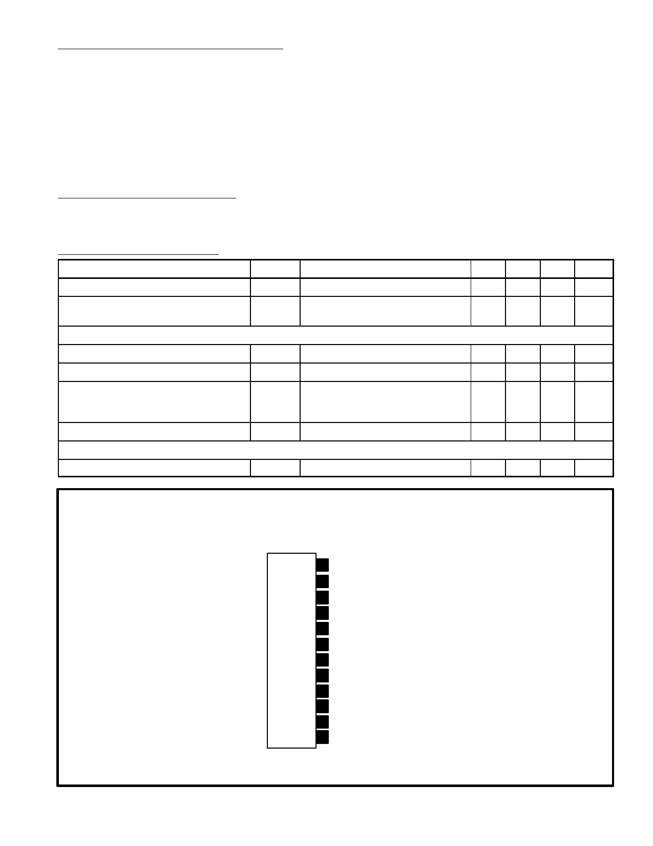
Pin Connection Diagram
(Front View)
12 TR1 Drain
11 TR1 Drain
10 No Pin
9 TR1 Source
8 TR1 Source
7 OCP Setting Level Input
6 Amplifier Circuit Control
5 TR1 Gate
4 Drive Voltage Input
3 GND
2 Error Detection Level
1 Vref (40.5V typ) Input
Share Link: 