SL311N 데이터 시트보기 (PDF) - System Logic Semiconductor
부품명
상세내역
일치하는 목록
SL311N Datasheet PDF : 2 Pages
| |||
SL311
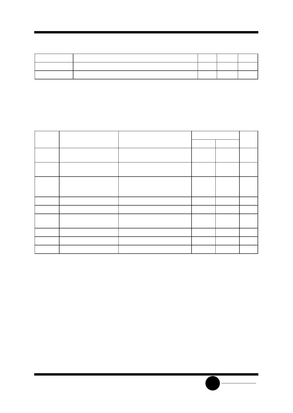
RECOMMENDED OPERATING CONDITIONS
Symbol
Parameter
VCC + VEE
TA
Total Supply Voltage
Operating Temperature, All Package Types
Min Max Unit
30
V
- 45
+85
°C
ELECTRICAL CHARACTERISTICS (VCC=+15 V, VEE= -15 V, TA =+25°C unless otherwise noted
[Note 1])
Symbol
Parameter
Test Conditions
Guaranteed Limits Unit
Min
Max
VIO Input Offset Voltage
(Note 2)
IIO Input Offset Current
(Note 2)
IIB Input Bias Current
RS ≤ 50 kΩ, TA = +25°C
RS ≤ 50 kΩ, -45°C ≤ TA ≤ 85°C
TA = +25°C
-45°C ≤ TA ≤ 85°C
TA = +25°C
TA = -45°C
TA = +85°C
7.5
mV
10
50
nA
100
250
nA
375
500
AV Voltage Gain
150000
tDLH Propagation Delay Time
VDS Saturation Voltage
TA = +25°C
VID ≤ -10 mV, IO=50 mA
300
ns
1.5
V
VIR Input Voltage Range
-14.5
13.0
V
ICC Positive Supply Current
+7.5
mA
IEE Negative Supply Current
-5.0
mA
NOTES:
1. Offset voltage, offset current and bias current specifications apply for a supply voltage range from a single
5.0 volt supply up to ±15 volt supplies.
2. The offset voltages and offset currents given are the maximum values required to drive the output within a volt
of either supply with a 1.0 mA load. Thus, these parameters define an error band and take into account the
“worst case” effects of voltage gain and input impedance.
SLS
System Logic
Semiconductor
Share Link: 