NTE956 데이터 시트보기 (PDF) - NTE Electronics
부품명
상세내역
일치하는 목록
NTE956 Datasheet PDF : 2 Pages
| |||
Electrical Characteristics: (0° ≤ TJ ≤ +125°C, VIN–VOUT = 5V, IO = 500mA, IMAX = 1.5A, Note 1
unless otherwise specified)
Parameter
Symbol
Test Conditions
Min Typ Max Unit
Line Regulation
Load Regulation
Regline TA = +25°C, 3V ≤ (VIN–VOUT) ≤ 40V, Note 2 –
3V ≤ (VIN–VOUT) ≤ 40V
–
Regload TA = +25°C,
10mA ≤ IO ≤ 1MAX,
Note 2
VOUT ≤ 5V
–
VOUT ≥ 5V
–
0.01 0.04 %/V
0.02 0.07 %/V
5
25 mV
0.1 0.5 %
Thermal Regulation
Adjustment Pin Current
Adjustment Pin Current
Change
10mA ≤ IO ≤ 1MAX, Note 2 VOUT ≤ 5V
–
VOUT ≥ 5V
–
TA = +25°C, 20ms Pulse
–
IAdj
–
∆IAdj 10mA ≤ IL ≤ IMAX, 2.5V ≤ (VIN–VOUT) ≤ 40V
–
20
70 mV
0.3 1.5 %
0.04 0.07 %/W
50 100 µA
0.2 5.0 µA
Reference Voltage
Temperature Stability
Minimum Load Current
Maximum Output Current
Limit
RMS Output Noise,
% of VOUT
Ripple Rejection Ratio
Long Term Stability
Vref 3V ≤ (VIN–VOUT) ≤ 40V, 10mA ≤ IO ≤ 1MAX, 1.20 1.25 1.30 V
P ≤ PMAX
TS 0° ≤ TJ ≤ +125°C
–
1
–
%
ILmin (VIN–VOUT) ≤ 40V
–
3.5 10 mA
Imax VIN–VOUT ≤ 15V
1.5 2.2
–
A
VIN–VOUT = 40V
–
0.4
–
A
N TA = +25°C, 10Hz ≤ f ≤ 10kHz
– 0.003 –
%
RR VOUT = 10V, f = 120Hz
–
65
– dB
CADJ = 10µF 66
80
– dB
S TA = +125°C, 1000 Hours
–
0.3 1.0 %
Note 1. Although power dissipation is internally limited, these specifications are applicable for power
dissipations of 20W.
Note 2. Regulation is measured at constant junction temperature, using pulse testing with a low duty
cycle. Changes in output voltage due to heating effects are covered under the specification
for thermal regulation.
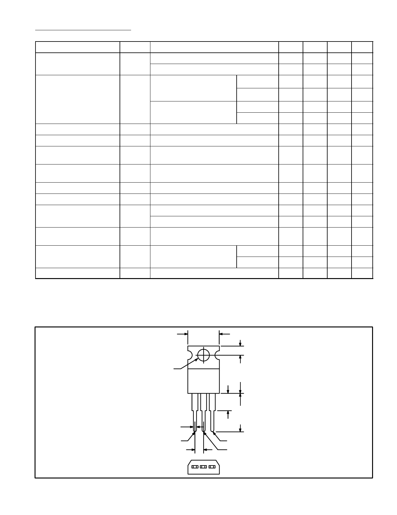
.420 (10.67)
Max
.110 (2.79)
.147 (3.75)
Dia Max
.500
(12.7)
Max
.070 (1.78)
Max
Adj
.100 (2.54)
.250
(6.35)
Max .500
(12.7)
Min
VIN
VOUT/Tab
Share Link: 