NTE7151 데이터 시트보기 (PDF) - NTE Electronics
부품명
상세내역
일치하는 목록
NTE7151 Datasheet PDF : 8 Pages
| |||
Absolute Maximum Ratings: (TA = +25°C unless otherwise specified)
Power Supply Voltage, VCC . . . . . . . . . . . . . . . . . . . . . . . . . . . . . . . . . . . . . . . . . . . . . . . . . . . . . . . . . . 12V
Power Dissipation, PDmax . . . . . . . . . . . . . . . . . . . . . . . . . . . . . . . . . . . . . . . . . . . . . . . . . . . . . . . . . 2.19W
Derate Above 25°C . . . . . . . . . . . . . . . . . . . . . . . . . . . . . . . . . . . . . . . . . . . . . . . . . . . . 17.5mW/°C
Input Terminal Voltage, Vin . . . . . . . . . . . . . . . . . . . . . . . . . . . . . . . . . . . . . . . . GND–0.3V to VCC+0.3V
Input Signal Amplitude, ein . . . . . . . . . . . . . . . . . . . . . . . . . . . . . . . . . . . . . . . . . . . . . . . . . . . . . . . . 4VP–P
Operating Temperature Range, Topr . . . . . . . . . . . . . . . . . . . . . . . . . . . . . . . . . . . . . . . . . –20° to +65°C
Storage Temperature Range, Tstg . . . . . . . . . . . . . . . . . . . . . . . . . . . . . . . . . . . . . . . . . . –55° to +150°C
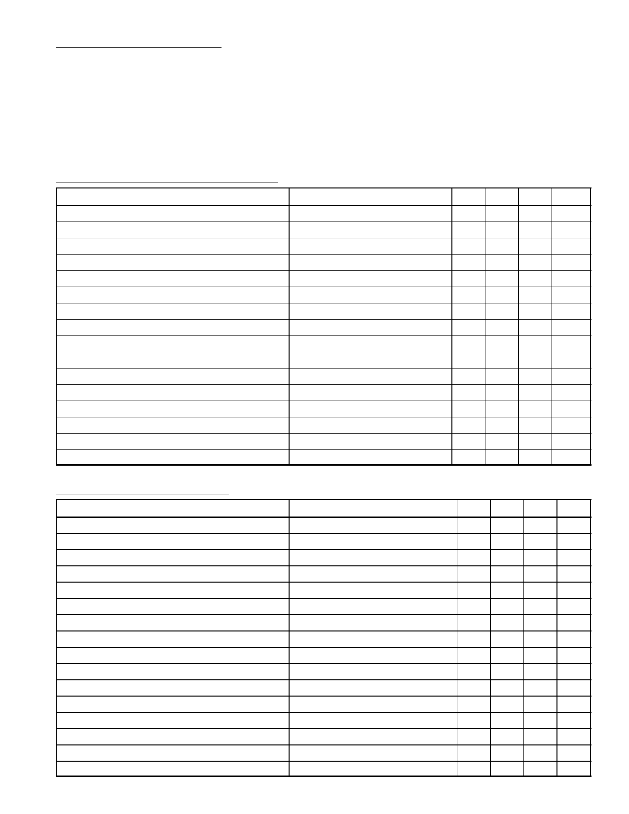
Recommended Operating Conditions:
Parameter
Symbol
Test Conditions
PIF Power Supply Voltage
SIF Power Supply Voltage
V/C/D Power Supply Voltage
H. VCC Power Supply Voltage
D. VCC Power Supply Voltage
TV External Video Input Level
Standard Video Input Level
Standard Chroma Input Level
FBP Width
FBP Input Flow In Current
PIF Output Load Resistor
SIF Output Load Resistor
RGB Output Load Resistor
Horizontal Output Load Resistor
Vertical Output Load Resistor
Sync.Separation Output Flow In Current
VCCP
VCCS
VCCV
H. VCC
D. VCC
Vin37/39
Vin43
Vin45
TFBP
IFBPmax
ROP
ROS
RORGB
RHOUT
RVOUT
Isyncmax
Including Sync.
Including Sync.
At Burst Signal
Vth = 1.4V, VCC = –1.4V
maximum 10mA
Min Typ Max Unit
8.5 9.0 9.5 V
8.5 9.0 9.5 V
8.5 9.0 9.5 V
8.5 9.0 9.5 V
2.7 3.3 3.8 V
– 1.0
– 1.0
– 286
10 12
–
VP–P
–
VP–P
– mVP–P
–
µs
–
–
2 mA
2.0 8.2 –
kΩ
1.0 8.2 –
kΩ
– 1.8 –
kΩ
330 800 –
Ω
4.1 5.7 –
kΩ
–
–
1 mA
DC Electrical Characteristics: (VCC = 9V, H. VCC = 9V, TA = +25°C unless otherwise specified)
Parameter
Symbol
Test Conditions
Min Typ Max Unit
Sound Output (Pin1)
Sound Output (Pin2)
RF AGC (Pin3)
AGC Filter (Pin5)
PIF GND (Pin6)
V1
V2
V3
V5
GND
3.2 3.7 4.2 V
3.2 3.7 4.2 V
– 0.0 0.5 V
7.0 7.5 8.0 V
– 0.0 –
V
PIF Input (Pin7)
PIF Input (Pin8)
PIF VCC (Pin9)
Loop Filter (Pin10)
APC Filter (Pin11)
VCXO (Pin12)
V/C/D GND (Pin13)
V7
V8
VCC
V10
V11
V12
GND
1.5 2.0 2.5 V
– 0.0 0.5 V
– 9.0 –
V
– 4.5 –
V
6.0 6.5 7.0 V
5.3 5.8 6.3 V
– 0.0 –
V
F–BLK (Pin14)
V14
Analog R Input (Pin15)
V15
Analog G Input (Pin16)
V16
Analog B Input (Pin17)
V17
– 0.0 –
V
4.4 4.9 5.4 V
4.4 4.9 5.4 V
4.4 4.9 5.4 V
Share Link: 