LA7583 데이터 시트보기 (PDF) - SANYO -> Panasonic
부품명
상세내역
일치하는 목록
LA7583 Datasheet PDF : 16 Pages
| |||
Continued from preceding page.
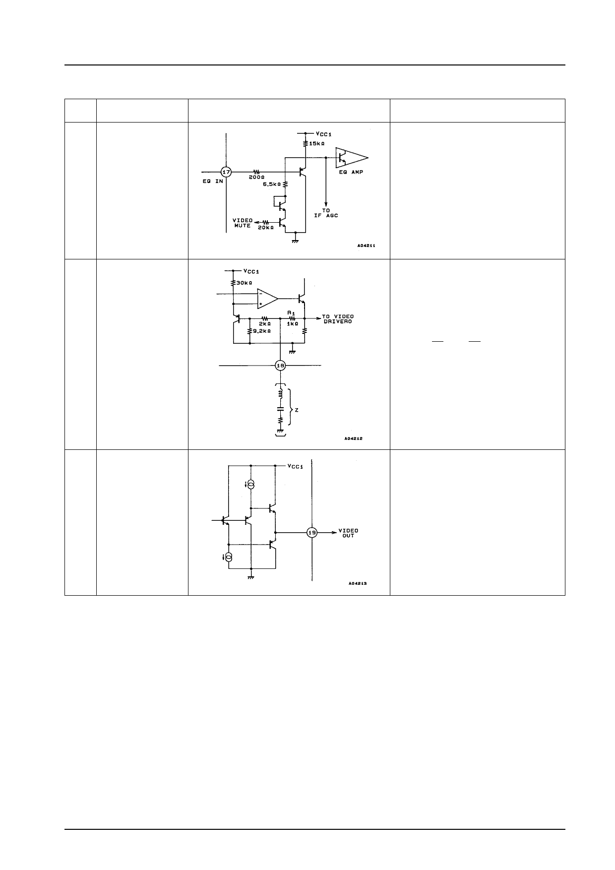
Pin
No.
Symbol
17 EQUALIZER INPUT
LA7583
Circuit Configuration
Description
Pin 17 is the equalizer amplifier input pin. A
signal which has passed through a 4.5 MHz
trap is input through pin 17 and is output
.through pin 19.
The input level of pin 17 is 1.5 Vp-p. This
is amplified 3 dB to 2 Vp-p by the
equalizer amplifier.
18 EQUALIZER FILTER
Pin 18 is the equalizer pin. The equalizer
amplifier is of the voltage follower type with
a voltage gain of 3 dB. To correct the
frequency characteristics, connect LCR
externally.
The operating characteristics are as follows:
Ve
R1
Av = = 1 + (times)
Vi
Z
19 EQUALIZER
OUTPUT
Pin 19 is the equalizer amplifier output pin.
This output has a built-in low-impedance
drive circuit.
Continued on next page.
No.5177-11/16
Share Link: 