HD74HC299 데이터 시트보기 (PDF) - Renesas Electronics
부품명
상세내역
일치하는 목록
HD74HC299 Datasheet PDF : 9 Pages
| |||
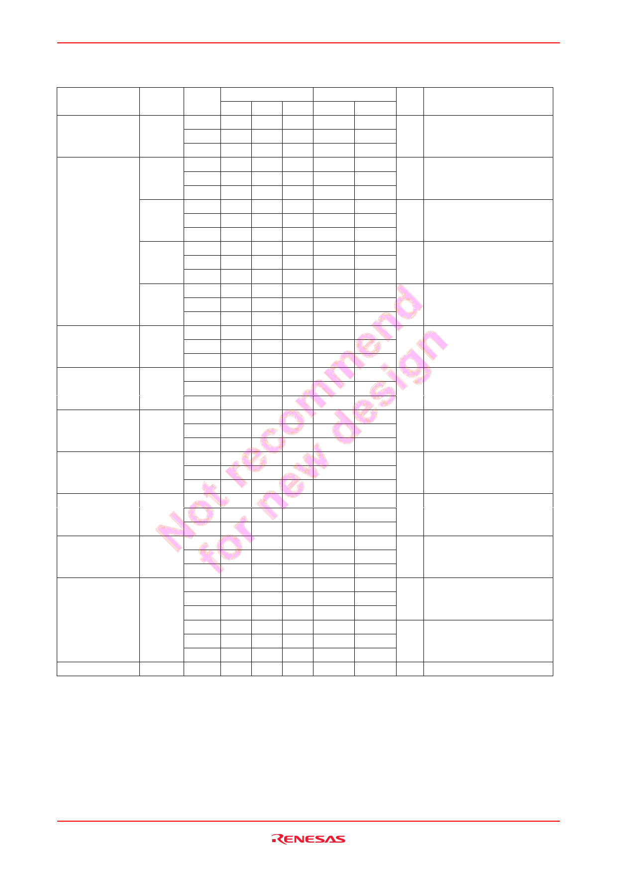
HD74HC299
Switching Characteristics
Item
Symbol VCC (V)
Maximum clock
frequency
fmax
2.0
4.5
6.0
Propagation delay tPLH
2.0
time
tPHL
4.5
6.0
tPHL
2.0
4.5
6.0
tPLH
2.0
tPHL
4.5
6.0
tPHL
2.0
4.5
6.0
Output enable time tZH
2.0
tZL
4.5
6.0
Output disable
time
tHZ
2.0
tLZ
4.5
6.0
Setup time
tsu
2.0
4.5
6.0
Hold time
th
2.0
4.5
6.0
Removal time
trem
2.0
4.5
6.0
Pulse width
tw
2.0
4.5
6.0
Output rise/fall
time
tTLH
2.0
tTHL
4.5
6.0
2.0
4.5
6.0
Input capacitance Cin
—
Ta = 25°C
Min Typ Max
—— 5
— — 25
— — 29
— — 190
— — 38
— — 32
— — 220
— — 44
— — 37
— — 190
— — 38
— — 32
— — 220
— — 44
— — 37
— — 160
— — 32
— — 27
— — 160
— — 32
— — 27
100 — —
20 — —
17 — —
5 ——
5 ——
5 ——
50 — —
10 — —
9 ——
80 — —
16 — —
14 — —
— — 60
— — 12
— — 10
— — 75
— — 15
— — 13
— 5 10
(CL = 50 pF, Input tr = tf = 6 ns)
Ta = –40 to +85°C
Unit
Min
Max
Test Conditions
—
4 MHz
—
20
—
23
—
240 ns Clock to QA’ or QH’
—
48
—
41
—
275 ns Clear to QA’ or QH’
—
55
—
47
—
240 ns Clock to QA – QH
—
48
—
41
—
275 ns Clear to QA – QH
—
55
—
47
—
200 ns
—
40
—
34
—
200 ns
—
40
—
34
125
—
ns Select
25
—
21
—
5
—
ns Select
5
—
5
—
65
—
ns Clear
13
—
11
—
100
—
ns
20
—
17
—
—
75
ns A/QA thru H/QH outputs
—
15
—
13
—
95
ns QA’ & QH’ outputs
—
19
—
16
—
10 pF
Rev.2.00 Jan 31, 2006 page 5 of 8
Share Link: 