HD74HC589 데이터 시트보기 (PDF) - Renesas Electronics
부품명
상세내역
일치하는 목록
HD74HC589
Renesas Electronics

HD74HC589 Datasheet PDF : 9 Pages
| |||
HD74HC589
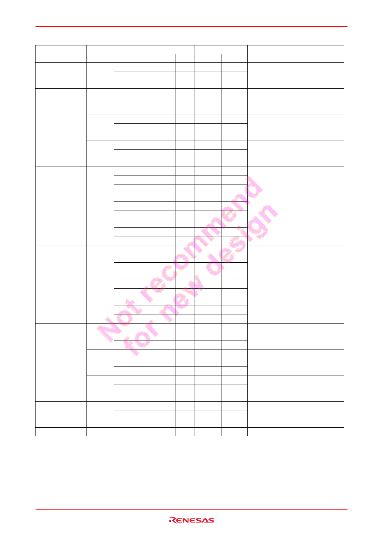
Switching Characteristics (CL = 50 pF, Input tr = tf = 6 ns)
Item
Maximum clock
frequency
Propagation delay
time
Output enable
time
Output disable
time
Pulse width
Setup time
Hold time
Output rise/fall
time
Input capacitance
Symbol VCC (V)
fmax
2.0
4.5
6.0
tPLH
2.0
tPHL
4.5
6.0
tPLH
2.0
tPHL
4.5
6.0
tPLH
2.0
tPHL
4.5
6.0
tZL
2.0
tZH
4.5
6.0
tLZ
2.0
tHZ
4.5
6.0
tw
2.0
4.5
6.0
tsu
2.0
4.5
6.0
tsu
2.0
4.5
6.0
tsu
2.0
4.5
6.0
th
2.0
4.5
6.0
th
2.0
4.5
6.0
th
2.0
4.5
6.0
tTLH
2.0
tTHL
4.5
6.0
Cin
—
Ta = 25°C
Min Typ Max
——
5
— — 27
— — 32
— — 200
— 20 40
— — 34
— — 175
— 15 35
— — 30
— — 175
— 16 35
— — 30
— — 150
— 9 30
— — 26
— — 150
— 14 30
— — 26
80 — —
16
8
—
14 — —
100 — —
20
1
—
17 — —
100 — —
20 — —
17 — —
100 — —
20 — —
17 — —
5 ——
5
0
—
5 ——
5 ——
5 ——
5 ——
5 ——
5 ——
5 ——
— — 75
— 5 15
— — 13
— 5 10
Ta = –40 to +85°C
Min
Max Unit
Test Conditions
—
4 MHz
—
21
—
25
—
250 ns Latch clock to QH
—
50
—
43
—
220 ns Shift clock to QH
—
44
—
37
—
220 ns Serial shift/parallel load to QH
—
44
—
37
—
190 ns
—
38
—
33
—
190 ns
—
38
—
33
100
—
ns
20
—
17
—
125
—
ns Data to latch clock
25
—
21
—
125
—
ns SA to shift clock
25
—
21
—
125
—
ns Serial shift/parallel load to
25
—
shift clock
21
—
5
—
ns Latch clock to data
5
—
5
—
5
—
ns Shift clock to SA
5
—
5
—
5
—
ns Shift clock to serial shift/
5
—
parallel load
5
—
—
95
ns
—
19
—
16
—
10
pF
Rev.2.00 Mar 30, 2006 page 5 of 8
Share Link: