CS8361 데이터 시트보기 (PDF) - Cherry semiconductor
부품명
상세내역
일치하는 목록
CS8361 Datasheet PDF : 6 Pages
| |||
Circuit Description
ENABLE Function
The ENABLE function switches the output transistor for
VTRK on and off. When the ENABLE lead voltage exceeds
1.4V(typ), VTRK turns off. This input has several hundred
millivolts of hysteresis to prevent spurious output activity
during power-up or power-down.
RESET Function
The RESET is an open collector NPN transistor, con-
trolled by a low voltage detection circuit sensing the VSTBY
(5V) output voltage. This circuit guarantees the RESET
output stays below 1V (0.1V typ) when VSTBY is as low as
1V to ensure reliable operation of microprocessor-based
systems.
VTRK Output Voltage
This output uses the same type of output device as VSTBY,
but is rated for 250mA. The output is configured as a
tracking regulator of the standby output. By using the
standby output as a voltage reference, giving the user an
external programming lead (Adj lead), output voltages
from 5V to 20V are easily realized. The programming is
done with a simple resistor divider (Figure 2), and follow-
ing the formula:
VTRK = VSTBY ´ (1 + R1/R2) + IAdj ´ R1
If another 5V output is needed, simply connect the Adj
lead to the VTRK output lead.
Application Notes
External Capacitors
Output capacitors for the CS8361 are required for stability.
Without them, the regulator outputs will oscillate. Actual
size and type may vary depending upon the application
load and temperature range. Capacitor effective series
resistance (ESR) is also a factor in the IC stability. Worst-
case is determined at the minimum ambient temperature
and maximum load expected.
Output capacitors can be increased in size to any desired
value above the minimum. One possible purpose of this
would be to maintain the output voltages during brief
conditions of negative input transients that might be char-
acteristic of a particular system.
Capacitors must also be rated at all ambient temperatures
expected in the system. To maintain regulator stability
down to -40ûC, capacitors rated at that temperature must
be used.
More information on capacitor selection for Smart
Regulatorsª is available in the Smart Regulator applica-
tion note, ÒCompensation for Linear Regulators.Ó
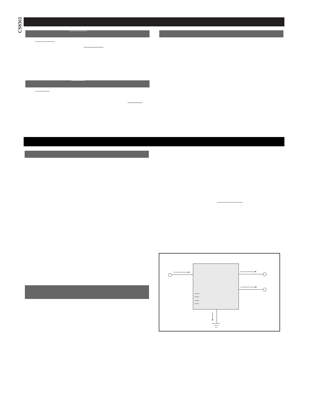
Calculating Power Dissipation
in a Dual Output Linear Regulator
The maximum power dissipation for a dual output regula-
tor (Figure 1) is:
PD(max) = {VIN(max)ÐVOUT1(min)}IOUT1(max)+
{VIN(max)ÐVOUT2(min)}IOUT2(max)+VIN(max)IQ (1)
Where
VIN(max) is the maximum input voltage,
VOUT1(min) is the minimum output voltage from VOUT1,
VOUT2(min) is the minimum output voltage from VOUT2,
IOUT1(max) is the maximum output current, for the
application
IOUT2(max) is the maximum output current, for the
application
IQ is the quiescent current the regulator consumes at
IOUT(max).
Once the value of PD(max) is known, the maximum per-
missible value of RQJA can be calculated:
RQJA =
150¡C - TA
PD
(2)
The value of RQJA can then be compared with those in
the package section of the data sheet. Those packages
with RQJA's less than the calculated value in equation 2
will keep the die temperature below 150¡C.
In some cases, none of the packages will be sufficient to
dissipate the heat generated by the IC, and an external
heat sink will be required.
IIN
VIN
Smart
Regulator
}Control
Features
IQ
IOUT1
IOUT2
VOUT1
VOUT2
Figure 1: Dual output regulator with key performance parameters
labeled.
4
Share Link: 