AMS1505V 데이터 시트보기 (PDF) - Advanced Monolithic Systems Inc
부품명
상세내역
일치하는 목록
AMS1505V Datasheet PDF : 8 Pages
| |||
AMS1505V
APPLICATION HINTS
3.3V
5V
CONTROL
POWER
SENSE
AMS1505V
OUTPUT
ADJ
R1
R2
RP
LOAD
RP
+
VOUT
-
Figure 2. Remote Load Sensing
VOUT
FIGURE 1
VOUT
FIGURE 2
(∆IOUT)(RP)
IOUT
TIME
Figure 3. Remote Sensing Improves Load Regulation
Voltage drops due to RP are not eliminated; they will add to the
dropout voltage of the regulator regardless of whether they are
inside or outside the regulation loop. The AMS1505V can control
the voltage at the load as long as the input-output voltage is
greater than the total of the dropout voltage of the device plus the
voltage drop across RP.
Stability
The circuit design used in the AMS1505V series requires the use
of an output capacitor as part of the device frequency
compensation. The addition of 150µF aluminum electrolytic or a
22µF solid tantalum on the output will ensure stability for all
operating conditions. For best frequency response use capacitors
with an ESR of less than 1Ω.
In order to meet the transient requirements of the processor larger
value capacitors are needed. Tight voltage tolerances are required
in the power supply. To limit the high frequency noise generated
by the processor high quality bypass capacitors must be used. In
order to limit parasitic inductance (ESL) and resistance (ESR) in
the capacitors to acceptable limits, multiple small ceramic
capacitors in addition to high quality solid tantalum capacitors are
required.
When the adjustment terminal is bypassed to improve the ripple
rejection, the requirement for an output capacitor increases. The
Adjust pin is brought out on the fixed voltage device specifically
to allow this capability. To ensure good transient response with
heavy load current changes capacitor values on the order of
100µF are used in the output of many regulators. To further
improve stability and transient response of these devices larger
values of output capacitor can be used.
The modern processors generate large high frequency current
transients. The load current step contains higher order frequency
components than the output coupling network must handle until
the regulator throttles to the load current level. Because they
contain parasitic resistance and inductance, capacitors are not
ideal elements. These parasitic elements dominate the change in
output voltage at the beginning of a transient load step change.
The ESR of the output capacitors produces an instantaneous step
in output voltage (∆V=∆I)(ESR). The ESL of the output
capacitors produces a droop proportional to the rate of change of
the output current (V= L)(∆I/∆t). The output capacitance
produces a change in output voltage proportional to the time until
the regulator can respond (∆V=∆t) (∆I/C). Figure 4 illustrates
these transient effects.
ESR
EFFECTS
ESL
EFFECTS
CAPACITANCE
EFFECTS
SLOPE, V/t = ∆I/C
POINT AT WHICH REGULATOR
TAKES CONTROL
Figure 4.
Output Voltage
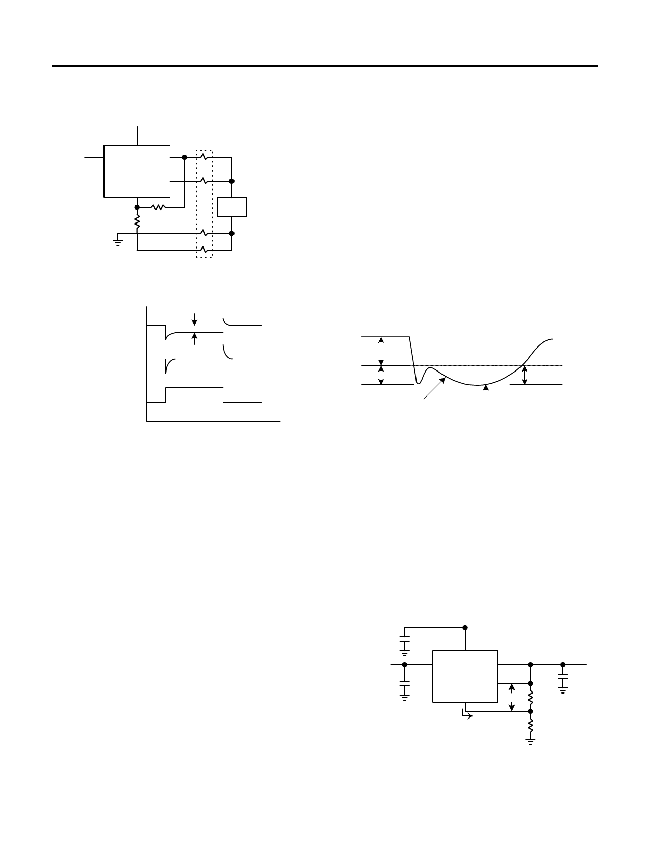
The AMS1505V series develops a 1.25V reference voltage
between the Sense pin and the Adjust pin (Figure5). Placing a
resistor between these two terminals causes a constant current to
flow through R1 and down through R2 to set the overall output
voltage. In general R1 is chosen so that this current is the
specified minimum load current of 10mA.The current out of the
Adjust pin is small, typically 50µA and it adds to the current
from R1. Because IADJ is very small it needs to be considered
only when very precise output voltage setting is required. For
best regulation the top of the resistor divider should be connected
directly to the Sense pin.
VCONTROL
+
VPOWER
+
CONTROL
POWER
OUTPUT
AMS1505V
SENSE
ADJ
IADJ
50µA
VREF
VOUT = VREF (1+ R2/R1)+IADJR2
+
R1
R2
VOUT
Figure 5. Setting Output Voltage
Advanced Monolithic Systems, Inc. 6680B Sierra Lane, Dublin, CA 94568 Phone (925) 556-9090 Fax (925) 556-9140
Share Link: 