MAX125ACAX 데이터 시트보기 (PDF) - Maxim Integrated
부품명
상세내역
일치하는 목록
MAX125ACAX Datasheet PDF : 16 Pages
| |||
2x4-Channel, Simultaneous-Sampling
14-Bit DAS
Table 1. Modes of Operation
A3
A2
A1
A0
0
0
0
0
0
0
0
1
0
0
1
0
0
0
1
1
0
1
0
0
0
1
0
1
0
1
1
0
0
1
1
1
1
X
X
X
X = Don’t care
CONVERSION
TIME (µs)
3
6
9
12
3
6
9
12
—
MODE
Input Mux A/Single-Channel Conversion (default at power-up)
Input Mux A/Two-Channel Conversion
Input Mux A/Three-Channel Conversion
Input Mux A/Four-Channel Conversion
Input Mux B/Single-Channel Conversion
Input Mux B/Two-Channel Conversion
Input Mux B/Three-Channel Conversion
Input Mux B/Four-Channel Conversion
Power-Down
TO DAC
MAX125
MAX126
REFOUT 7 (2.5V)
AV = 1
REFIN
6 (2.5V)
4.7µF
0.1µF
10k
2.5V
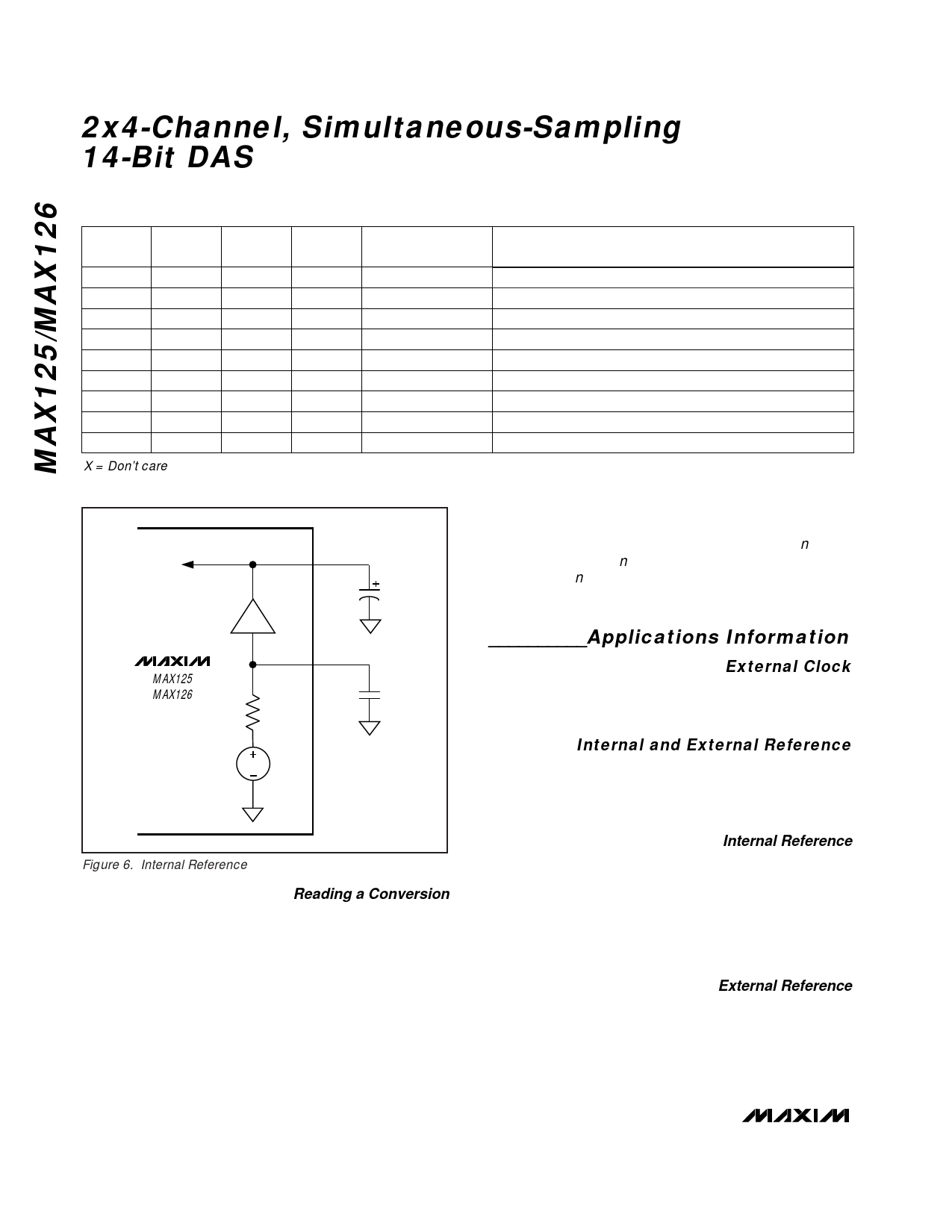
Figure 6. Internal Reference
Reading a Conversion
Digitized data from up to four channels are stored in
memory to be read out through the parallel interface.
After receiving an INT signal, the user can access up to
four conversion results by performing up to four read
operations.
With CS low, the conversion result from CH_1 is
accessed, and INT is reset high on the first RD falling
edge. On the RD rising edge, the internal address
pointer is advanced. If a single conversion is pro-
grammed, only one RD pulse is required, and the
address pointer is reset to CH_1. For multichannel con-
versions, up to four RD falling edges sequentially
access the data for channels 1 through 4. For n chan-
nels converted (1 < n ≤ 4), the address pointer is reset
to CH_1 after n RD pulses. Do not perform a read oper-
ation during conversion, as it will corrupt the conver-
sion’s accuracy.
__________Applications Information
External Clock
The MAX125/MAX126 require a TTL-compatible clock
up to 16MHz for proper operation. The clock duty
cycle’s range is between 30% and 70%.
Internal and External Reference
The MAX125/MAX126 can be used with an internal or
external reference voltage. An external reference can
be connected directly at REFIN. An internal buffer with
a gain of +1 provides 2.5V at REFOUT.
Internal Reference
The full-scale range with the internal reference is ±5V
for the MAX125 and ±2.5V for the MAX126. Bypass
REFIN with a 0.1µF capacitor to AGND and bypass the
REFOUT pin with a 4.7µF (min) capacitor to AGND
(Figure 6). The maximum value to compensate the ref-
erence buffer is 22µF. Larger values are acceptable if
low-ESR capacitors are used.
External Reference
For operation over a wide temperature range, an exter-
nal 2.5V reference with tighter specifications improves
accuracy. The MAX6325 is an excellent choice
to match the MAX125/MAX126 accuracy over the
commercial and extended temperature ranges with a
10 ______________________________________________________________________________________
Share Link: 