LT1680 데이터 시트보기 (PDF) - Linear Technology
부품명
상세내역
일치하는 목록
LT1680 Datasheet PDF : 16 Pages
| |||
LT1680
APPLICATIONS INFORMATION
additional current can be minimized by making the con-
nection through an external resistor (100k is typically used).
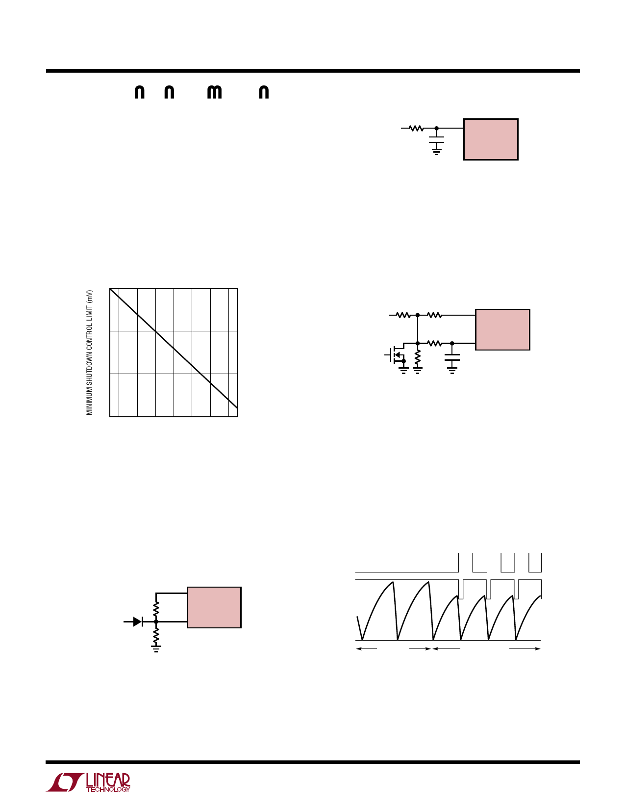
When shutting down the LT1680, the RUN/SHDN pin volt-
age must remain between the shutdown threshold (~1.13V)
and a minimum shutdown control limit voltage (see Fig-
ure 4) for a least 25µs. If a digital input or fast moving
clamp is used, this can be achieved by forcing a shutdown
control voltage above the minimum limit or by using a
simple integrator to increase the fall time of the input sig-
nal. A single pole integrator stage must have a
τ ≥ (7)(10 –5).
800
700
600
500
– 40 – 20 0 20 40 60
TEMPERATURE (°C)
80
1680 F04
Figure 4. Minimum Shutdown Control Limit vs Temperature
Figure 5 is an example of a digital control input clamp. A
logic high signal pulls the RUN/SHDN pin above its turn-
on threshold through the diode. When a shutdown (logic
low) signal is received, the RUN/SHDN pin is forced to
0.95V via the resistor divider until shutdown is fully estab-
lished and the 5VREF voltage collapses.
R1
1N914 43k
DIGITAL
INPUT
R2
10k
5VREF
LT1680
RUN/SHDN
1680 F05
Figure 5. Digital Input Shutdown Level Control
Figure 6 is an example of a digital control integration stage
at the RUN/SHDN input. The integrator has a τ = (10)(103)
• (10)(10–9) = (1.0)(10–4). This circuit technique, however,
delays initiation of controller shutdown about 125µs from
the reception of the shutdown signal (5V – 0V transition).
R1
DIGITAL 10k
INPUT
RUN/SHDN
C1
10nF
LT1680
1680 F06
Figure 6. Digital Input Shutdown Integration Control
Figure 7 is an example of an integrator stage coupled with
a 24V input power supply sequencing circuit similar to that
shown in Figure 3. The integrator stage allows use of an
active shutdown clamp for implementation of both user-
controlled shutdown and input power supply sequencing
protection.
R1
VIN 160k
24V
R3
390k
R4
10k
SHDN
R2
10k
5VREF
LT1680
RUN/SHDN
C1
10nF
1680 F07
Figure 7. Input Supply Sequencing with
User-Controlled Shutdown
Oscillator Synchronization
The LT1680 oscillator generates a modified sawtooth
waveform at the CT pin between low and high thresholds
of 0.8V (vl) and 2.5V (vh) respectively. The oscillator can
be synchronized by driving a TTL level pulse into the SYNC
pin. This pin connects to a one shot circuit that reduces the
oscillator high threshold to 2V for about 200ns. The SYNC
input signal should have minimum on/off times of ≥1µs.
SYNC
2.5V
(vh)
2V
VCT
0.8V
FREE RUN
SYNCHRONIZED
(vl)
1680 F08
Figure 8. Free Run and Synchronized Oscillator
Waveforms (at CT Pin)
Inductor Selection
The inductor for an LT1680 converter is selected based on
output power, operating frequency and efficiency require-
11
Share Link: 