W6662CF 데이터 시트보기 (PDF) - Winbond
부품명
상세내역
일치하는 목록
W6662CF Datasheet PDF : 19 Pages
| |||
Preliminary W6662CF
SEL1 = 0, SEL0 = 1 is red channel of gain register and offset register selected.
SEL1 = 1, SEL0 = 0 is green channel of gain register and offset register selected.
SEL1 = 1, SEL0 = 1 is blue channel of gain register and offset register selected.
SEL1 = 0, SEL0 = 0 is reserved.
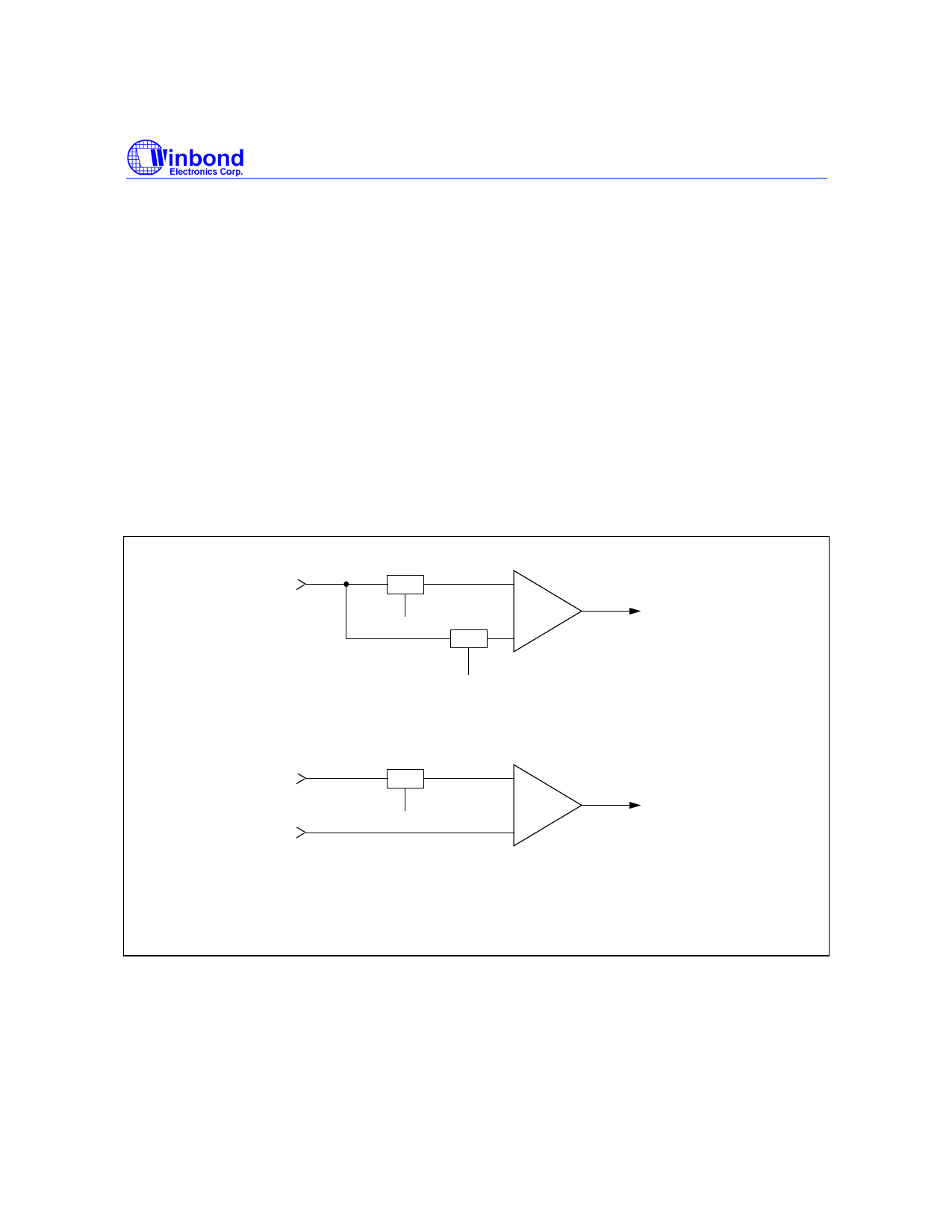
6.3 CDS vs S&H Mode
"CDS" stands for "correlated double sampling". It is used to reduce noise generated in CCD source
and to decrease the sampling error which induced from clampping voltage error. CDS takes two step
to sample a CCD's output pixel. In the first step, the reset level of CCD output is sampled and hold by
S/H1 at the falling edge of CDSCK1 signal. In the second step, the data signal of CCD output is
sampled and hold by S/H2 at the falling edge of CDSCK2 signal. The CDS output voltage is obtained
from the voltage difference of the outputs of S/H1 and S/H2.
In S&H mode, the data signal of CIS output is sampled and hold by S/H1 at the falling edge of
CDSCK2 signal and the output voltage is obtained from the voltage difference of the outputs of S/H1
and CISREF pin. Figure 6-3 shows the equivalent circuits of CDS and S&H mode processing.
From
I/P
MUX
S/H1
+
CDSCK1
S/H2
-
(a) CDS Mode.
CDSCK2
To
Gain/Offset
Adjust
From
I/P
MUX
From
CISREF
pin
S/H1
+
CDSCK2
-
(b) S&H Mode.
To
Gain/Offset
Adjust
Fig. 6-3 The Equivalent Circuit of CDS and S&H Mode.
6.4 Gain/Offset Adjustment
The analog input signal after CDS or S&H processed is amplified by PGA gain adjustment and then
shifted by offset value. The offset value will not affected by the PGA gain adjustment.
-6-
Share Link: 