W134SHT 데이터 시트보기 (PDF) - Cypress Semiconductor
부품명
상세내역
일치하는 목록
W134SHT Datasheet PDF : 12 Pages
| |||
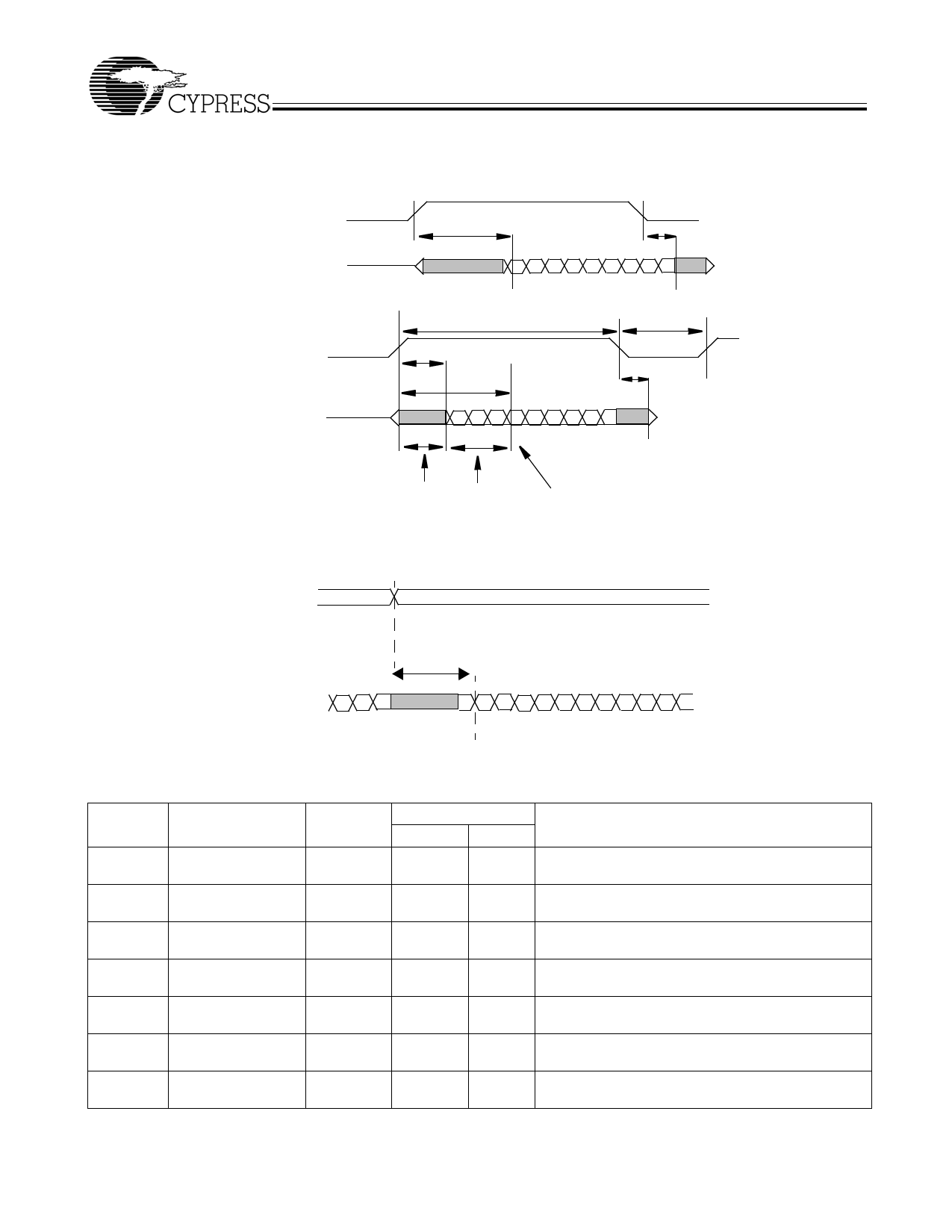
Timing Diagrams
Power-down Exit and Entry
PwrDnB
Clk/ClkB
Output Enable Control
StopB
Clk/ClkB
tPOWERUP
tON
tCLKON
tCLKSETL
W134M/W134S
tPOWERDN
tSTOP
tCLKOFF
Mult0 and/or Mult1
Output clock
not specified
glitches may
Clock enabled
and glitch-free
occur
Clock output settled within
50 ps of the phase before
disabled
Figure 5. State Transition Timing Diagrams
tMULT
Clk/ClkB
Figure 6. Multiply Transition Timing
Table 8. State Transition Latency Specifications
Transition
A
C
K
G
H
M
J
From
Power-down
Power-down
Power-down
VDD ON
VDD ON
VDD ON
Normal
To
Normal
Clk Stop
Test
Normal
Clk Stop
Test
Normal
Transition Latency
Parameter Max.
Description
tPOWERUP
tPOWERUP
3 ms
3 ms
Time from PwrDnB to Clk/ClkB output settled
(excluding tDISTLOCK).
Time from PwrDnB until the internal PLL and clock has
turned ON and settled.
tPOWERUP
tPOWERUP
tPOWERUP
3 ms
3 ms
3 ms
Time from PwrDnB to Clk/ClkB output settled
(excluding tDISTLOCK).
Time from VDD is applied and settled until Clk/ClkB
output settled (excluding tDISTLOCK).
Time from VDD is applied and settled until internal PLL
and clock has turned ON and settled.
tPOWERUP 3 ms Time from VDD is applied and settled until internal PLL
and clock has turned ON and settled.
tMULT
1 ms Time from when Mult0 or Mult1 changed until Clk/ClkB
output resettled (excluding tDISTLOCK).
Document #: 38-07426 Rev. *C
Page 6 of 12
Share Link: 