W134SHT(2003) 데이터 시트보기 (PDF) - Cypress Semiconductor
부품명
상세내역
일치하는 목록
W134SHT Datasheet PDF : 12 Pages
| |||
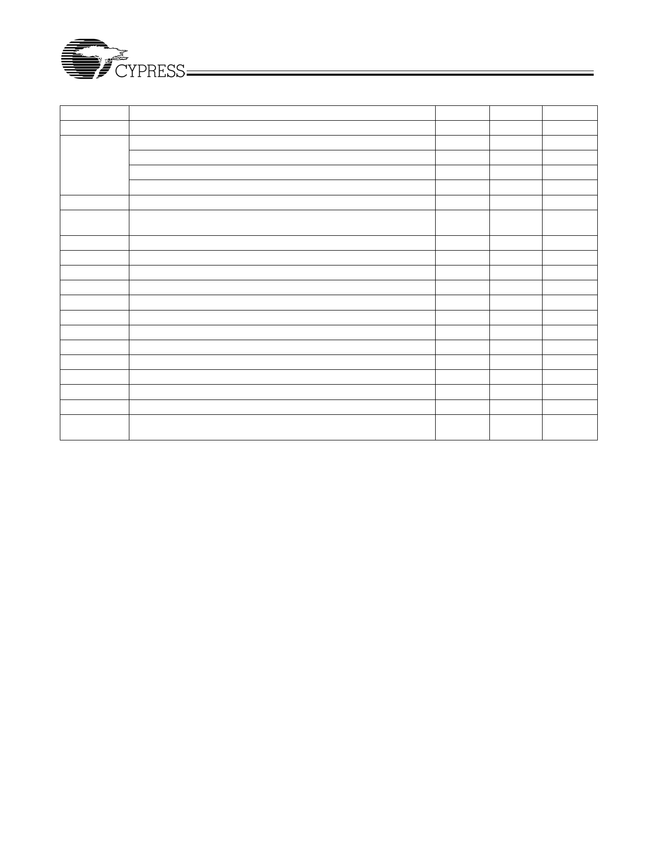
W134M/W134S
Device Characteristics
Parameter
tCYCLE
tJ
tSTEP
tERR,PD
tERR,SSC
VX,STOP
VX
VCOS
VOH
VOL
rOUT
IOZ
IOZ,STOP
DC
tDC,ERR
tR,tF
tCR,CF
Description
Clock Cycle Time
Cycle-to-Cycle Jitter at Clk/ClkB[9]
Total Jitter over 2, 3, or 4 Clock Cycles[9]
266-MHz Cycle-to-Cycle Jitter[10]
266-MHz Total Jitter over 2, 3, or 4 Clock Cycles[10]
Phase Aligner Phase Step Size (at Clk/ClkB)
Phase Detector Phase Error for Distributed Loop Measured at
PclkM-SynclkN (rising edges) (does not include clock jitter)
PLL Output Phase Error when Tracking SSC
Output Voltage during Clk Stop (StopB=0)
Differential Output Crossing-Point Voltage
Output Voltage Swing (p-p single-ended)[11]
Output High Voltage
Output Low voltage
Output Dynamic Resistance (at pins)[12]
Output Current during Hi-Z (S0 = 0, S1 = 1)
Output Current during Clk Stop (StopB = 0)
Output Duty Cycle over 10,000 Cycles
Output Cycle-to-Cycle Duty Cycle Error
Output Rise and Fall Times (measured at 20%–80% of output voltage)
Difference between Output Rise and Fall Times on the Same Pin of a
Single Device (20%–80%)
Notes:
9. Output Jitter spec measured at tCYCLE = 2.5 ns.
10. Output Jitter Spec measured at tCYCLE = 3.75 ns.
11. VCOS = VOH–VOL.
12. rOUT = DVO/ D IO. This is defined at the output pins.
Min.
2.5
–
–
–
–
1
–100
–100
1.1
1.3
0.4
–
1.0
12
–
–
40
–
250
–
Max.
3.75
60
100
100
160
–
100
100
2.0
1.8
0.6
2.0
–
50
50
500
60
50
500
100
Unit
ns
ps
ps
ps
ps
ps
ps
ps
V
V
V
V
V
Ω
µA
µA
%tCYCLE
ps
ps
ps
Document #: 38-07426 Rev. *B
Page 9 of 12
Share Link: 