V61C31161024-12K 데이터 시트보기 (PDF) - Mosel Vitelic Corporation
부품명
상세내역
일치하는 목록
V61C31161024-12K Datasheet PDF : 10 Pages
| |||
MOSEL VITELIC
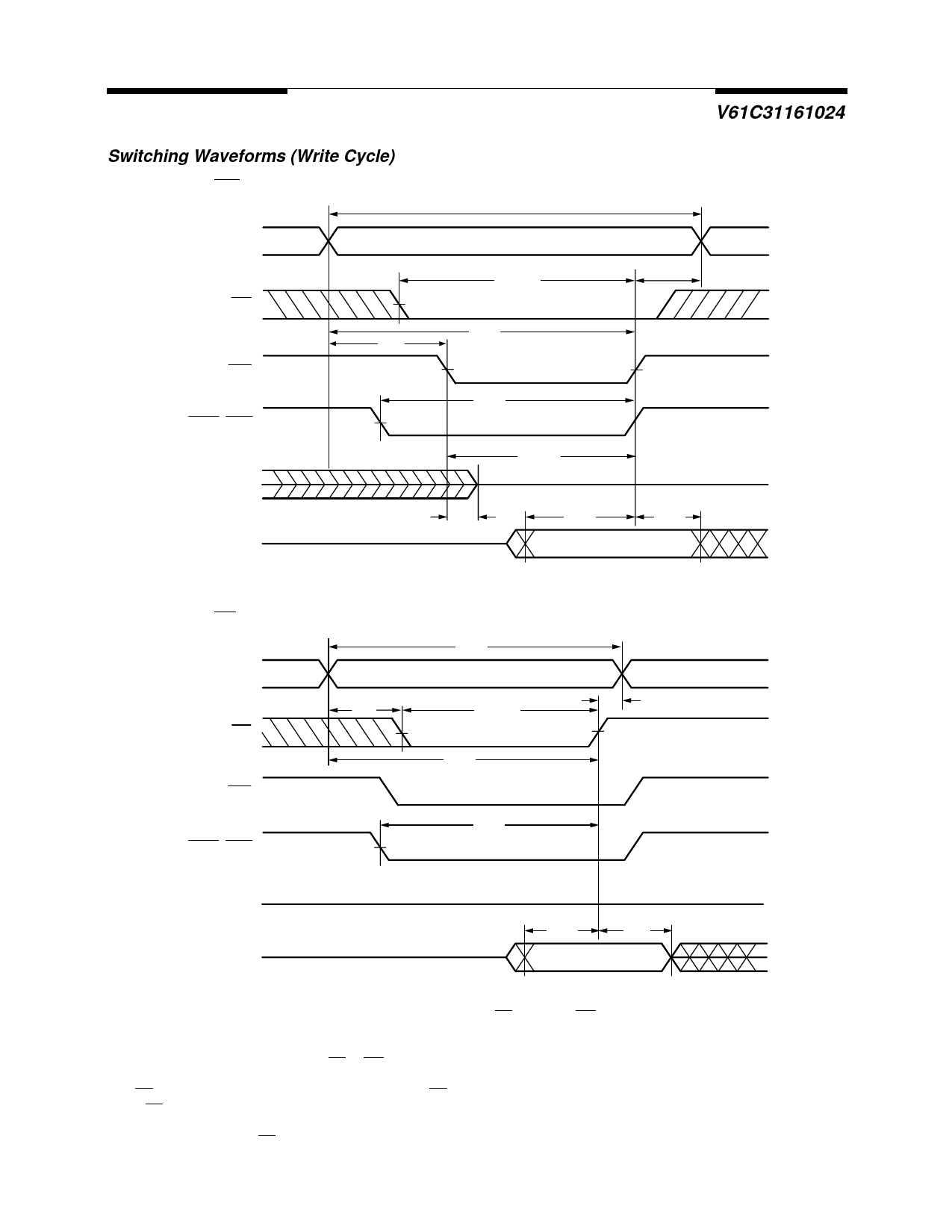
Switching Waveforms (Write Cycle)
Write Cycle 1 (WE Controlled)(4)
ADDRESS
CE
WE
UBE, LBE
OUTPUT
INPUT
tAS
tWHZ(3)
tWC
tCW(6)
tAW
tBW
tWP(1)
tDW
V61C31161024
tAH (2)
tDH
6131161024-09
Write Cycle 2 (CE Controlled)(4)
ADDRESS
tAS
CE
WE
UBE, LBE
tWC
tCW(6)
tAW
tBW
tAH (2)
Hi-Z
OUTPUT
INPUT
tDW
tDH
(5)
6131161024-10
NOTES:
1. The internal write time of the memory is defined by the overlap of CE active and WE low. All signals must be active to initiate and
any one signal can terminate a write by going inactive. The data input setup and hold timing should be referenced to the second
transition edge of the signal that terminates the write.
2. tAH is measured from the earlier of CE or WE going high.
3. During this period, I/O pins are in the output state so that the input signals of opposite phase to the outputs must not be applied.
4. OE = VIL or VIH. However it is recommended to keep OE at VIH during write cycle to avoid bus contention.
5. If CE is LOW during this period, I/O pins are in the output state. Then the data input signals of opposite phase to the outputs must
not be applied to them.
6. tCW is measured from CE going low to the end of write.
V61C31161024 Rev. 0.5 August 1999
7
Share Link: 