TDA9859 데이터 시트보기 (PDF) - NXP Semiconductors.
부품명
상세내역
일치하는 목록
TDA9859 Datasheet PDF : 20 Pages
| |||
Philips Semiconductors
Universal hi-fi audio processor for TV
Preliminary specification
TDA9859
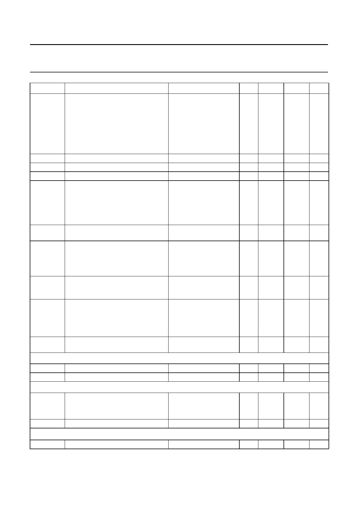
SYMBOL
PARAMETER
CONDITIONS
∆V15,18
maximum DC offset voltage between
adjoining step and any step to mute
Ro
Ro(L)
Co(L)
Vno(W)
for volume control
for bass control
for treble control
output resistance
allowed output load resistor
allowed output load capacitor
weighted noise voltage at output
(quasi-peak level)
B−1 dB
−1 dB bandwidth for loudspeaker
channel
Gv = 0 to +15 dB/mute
Gv = −64 to 0 dB/mute
Gv = 0 to +15 dB/mute
Gv = −12 to 0 dB/mute
Gv = −12 to +12 dB/mute
CCIR 468-3 weighted
Gv = +15 dB
Gv = 0 dB
Gv = −40 dB
Gv = −80 dB (mute)
THD
αcs(l-r)
αct(bus)
total harmonic distortion
for Vi(rms) = 0.2 V
for Vi(rms) = 1 V
for Vi(rms) = 2 V
stereo channel separation
crosstalk from I2C-bus to AF outputs
αbus = 20 log V--V---b-o-u--(-s-r-(m--p---s--p)--) (Vbus = spurious
I2C-bus signal voltage on AF output).
f = 20 to 12500 Hz
Gv = −30 to +15 dB
Gv = −30 to 0 dB
Gv = −30 to −6 dB
f = 10 kHz; Gv = 0 dB;
opposite input grounded
by 1 kΩ resistor
Gv = 0 dB
PSRR100
power supply ripple rejection with
100 Hz ripple
Gv = 0 dB;
VR(rms) < 200 mV
SCART output (pins 7 and 26)
Vo(max)(rms) maximum output signal (RMS value)
Ro(L)
output load resistor
THD ≤ 0.5%; RL > 5 kΩ
Power-on reset
VPONR
increasing supply voltage
start of reset
end of reset
VPONR
decreasing supply voltage start of reset
I2C-bus, SCL and SDA (pins 16 and 17)
VIH
HIGH-level input voltage
MIN. TYP.
−
2
−
0.5
−
2
−
0.5
−
0.5
−
−
10 −
−
−
−
102
−
32
−
27
−
20
20 −
−
0.1
−
0.1
−
0.1
−
75
−
100
−
55
2
−
5
−
−
−
5.2 6.0
4.4 5.2
3
−
MAX.
15
10
15
10
10
100
−
1.5
−
−
−
−
20 000
0.3
0.3
0.3
−
−
−
−
−
2.5
6.8
6.0
VP
UNIT
mV
mV
mV
mV
mV
Ω
kΩ
nF
µV
µV
µV
µV
Hz
%
%
%
dB
dB
dB
V
kΩ
V
V
V
V
1997 Sep 01
8
Share Link: 