MT5C2565 데이터 시트보기 (PDF) - Austin Semiconductor
부품명
상세내역
일치하는 목록
MT5C2565 Datasheet PDF : 11 Pages
| |||
Austin Semiconductor, Inc.
SRAM
MT5C2565
AC TEST CONDITIONS
Input pulse levels ...................................... Vss to 3.0V
Input rise and fall times ......................................... 5ns
Input timing reference levels ................................ 1.5V
Output reference levels ....................................... 1.5V
Output load ................................. See Figures 1 and 2
Q
255
+5V
480
Q
30pF
255
+5V
480
5 pF
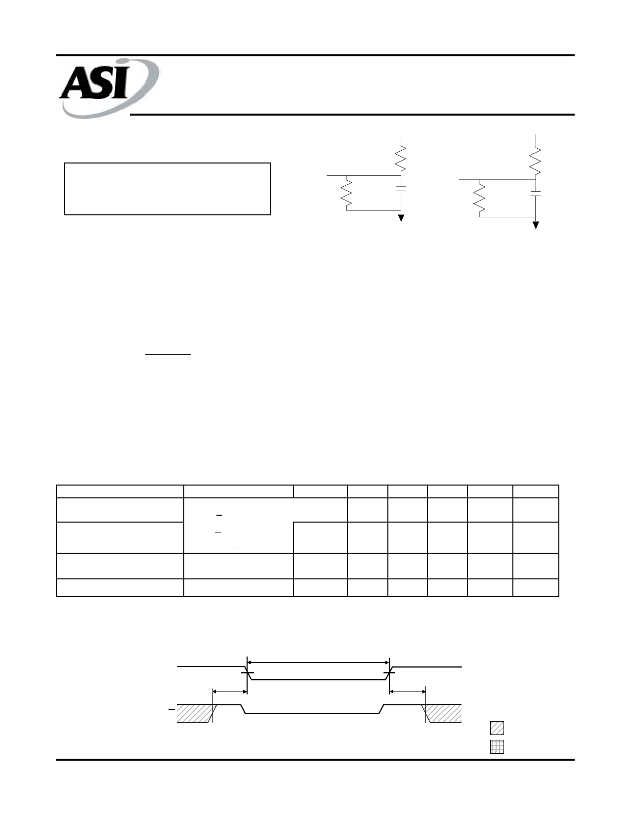
Fig. 1 Output Load
Equivalent
Fig. 2 Output Load
Equivalent
NOTES
1. All voltages referenced to VSS (GND).
2. -3V for pulse width < 20ns
3. ICC is dependent on output loading and cycle rates.
The specified value applies with the outputs
unloaded, and f = 1 Hz.
tRC (MIN)
4. This parameter is guaranteed but not tested.
5. Test conditions as specified with the output loading
as shown in Fig. 1 unless otherwise noted.
6. tHZCE, tHZOE and tHZWE are specified with CL = 5pF as
in Fig. 2. Transition is measured ±500mV typical from
steady state voltage, allowing for actual tester RC time
constant.
7. At any given temperature and voltage condition,
tHZCE is less than tLZCE, and tHZWE is less than tLZWE and
tHZOE is less than tLZOE.
8. WE\ is HIGH for READ cycle.
9. Device is continuously selected. Chip enable is held in
its active state.
10. Address valid prior to, or coincident with, latest
occurring chip enable.
11. tRC = Read Cycle Time.
12. Chip enable (CE\) and write enable (WE\) can initiate and
terminate a WRITE cycle.
DATA RETENTION ELECTRICAL CHARACTERISTICS (L Version Only)
DESCRIPTION
CONDITIONS
SYM MIN MAX UNITS NOTES
VCC for Retention Data
CE\ > (VCC - 0.2V)
VDR
2
---
V
Data Retention Current
VIN > (VCC - 0.2V)
or < 0.2V
VCC = 2V ICCDR
1
mA
*
Chip Deselect to Data
Retention Time
Operation Recovery Time
*for -25 and slower only
tCDR
0
---
tR
tRC
ns
4
ns
4, 11
LOW Vcc DATA RETENTION WAVEFORM
MT5C2565
Rev. 1.5 1/01
VCC
tCDR
CE\
VIH
VIL
11112222333344445555666677778888
DATA RETENTION MODE
4.5V
VDR > 2V
4.5V
VDR
tR
11112222333344445555111166662222777733331111888844222244
111122223333DON’T CARE
1111222233334444UNDEFINED
Austin Semiconductor, Inc. reserves the right to change products or specifications without notice.
5
Share Link: 