MC74HCT573ADTR2G 데이터 시트보기 (PDF) - ON Semiconductor
부품명
상세내역
일치하는 목록
MC74HCT573ADTR2G
ON Semiconductor

MC74HCT573ADTR2G Datasheet PDF : 6 Pages
| |||
MC74HCT573A
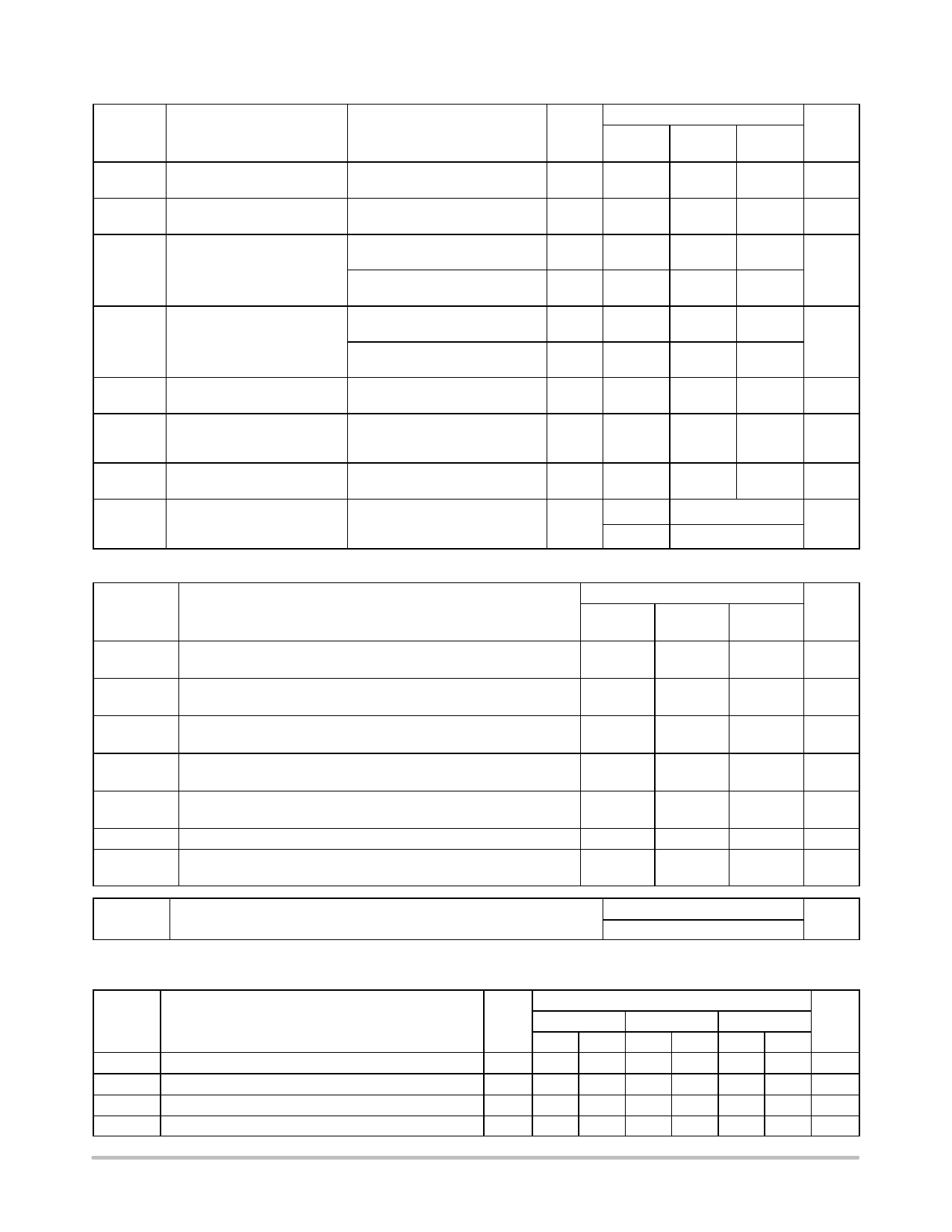
DC ELECTRICAL CHARACTERISTICS (Voltages Referenced to GND)
Symbol
VIH
VIL
VOH
Parameter
Minimum High−Level Input
Voltage
Maximum Low−Level Input
Voltage
Minimum High−Level Output
Voltage
VOL
Maximum Low−Level Output
Voltage
Iin
IOZ
ICC
ΔICC
Maximum Input Leakage
Current
Maximum Three−State
Leakage Current
Maximum Quiescent Supply
Current (per Package)
Additional Quiescent Supply
Current
Test Conditions
Vout = 0.1 V or VCC – 0.1 V
|Iout| ≤ 20 mA
Vout = 0.1 V or VCC – 0.1 V
|Iout| ≤ 20 mA
Vin = VIH or VIL
|Iout| ≤ 20 mA
Vin = VIH or VIL
|Iout| ≤ 6.0 mA
Vin = VIH or VIL
|Iout| ≤ 20 mA
Vin = VIH or VIL
|Iout| ≤ 6.0 mA
Vin = VCC or GND
Output in High−Impedance State
Vin = VIL or VIH
Vout = VCC or GND
Vin = VCC or GND
Iout ≤ 0 mA
Vin = 2.4 V, Any One Input
Vin = VCC or GND, Other Inputs
lout = 0 mA
Guaranteed Limit
VCC
–55 to
V
25_C
≤ 85_C ≤ 125_C Unit
4.5
2.0
2.0
2.0
V
5.5
2.0
2.0
2.0
4.5
0.8
0.8
0.8
V
5.5
0.8
0.8
0.8
4.5
4.4
4.4
4.4
V
5.5
5.4
5.4
5.4
4.5
3.98
3.84
3.7
4.5
0.1
0.1
0.1
V
5.5
0.1
0.1
0.1
4.5
0.26
0.33
0.4
5.5
±0.1
±1.0
±1.0
mA
5.5
±0.5
±5.0
±10
mA
5.5
4.0
40
160
mA
≥ –55_C
25_C to 125_C
5.5
2.9
2.4
mA
AC ELECTRICAL CHARACTERISTICS (VCC = 5.0 V ±10%, CL = 50 pF, Input tr = tf = 6.0 ns)
Guaranteed Limit
Symbol
Parameter
–55 to
25_C
≤ 85_C
≤ 125_C
Unit
tPLH,
tPHL
Maximum Propagation Delay, Input D to Output Q
(Figures 1 and 5)
30
38
45
ns
tPLH
Maximum Propagation Delay, Latch Enable to Q
tPHL
(Figures 2 and 5)
30
38
45
ns
TPLZ,
TPHZ
Maximum Propagation Delay, Output Enable to Q
(Figures 3 and 6)
28
35
42
ns
tTZL,
Maximum Propagation Delay, Output Enable to Q
tTZH
(Figures 3 and 6)
28
35
42
ns
tTLH,
tTHL
Maximum Output Transition Time, any Output
(Figures 1 and 5)
12
15
18
ns
Cin
Maximum Input Capacitance
Cout
Maximum Three−State Output Capacitance
(Output in High−Impedance State)
10
10
10
pF
15
15
15
pF
Typical @ 25°C, VCC = 5.0 V
CPD
Power Dissipation Capacitance (Per Enabled Output)*
48
pF
* Used to determine the no−load dynamic power consumption: PD = CPD VCC2f + ICC VCC.
ÎÎÎÎÎÎÎÎÎÎÎÎÎÎÎÎÎÎÎÎÎÎÎÎÎÎÎÎÎÎÎÎÎÎÎÎÎÎÎÎÎÎÎÎÎÎÎÎÎÎÎÎÎÎÎÎÎÎÎÎÎÎÎÎÎÎ TIMING REQUIREMENTS (VCC = 5.0 V ±10%, CL = 50 pF, Input tr = tf = 6.0 ns)
Guaranteed Limit
–55 to 25_C
≤ 85_C
≤ 125_C
Symbol
Parameter
Fig. Min Max Min Max Min Max Unit
tsu
Minimum Setup Time, Input D to Latch Enable
4
10
13
15
ns
th
Minimum Hold Time, Latch Enable to Input D
4
5.0
5.0
5.0
ns
tw
Minimum Pulse Width, Latch Enable
2
15
19
22
ns
tr, tf Maximum Input Rise and Fall Times
1
500
500
500 ns
http://onsemi.com
3
Share Link: