ICS9248G-143-T 데이터 시트보기 (PDF) - Integrated Circuit Systems
부품명
상세내역
일치하는 목록
ICS9248G-143-T
ICS9248G-143-T Datasheet PDF : 16 Pages
| |||

ICS9248 - 143
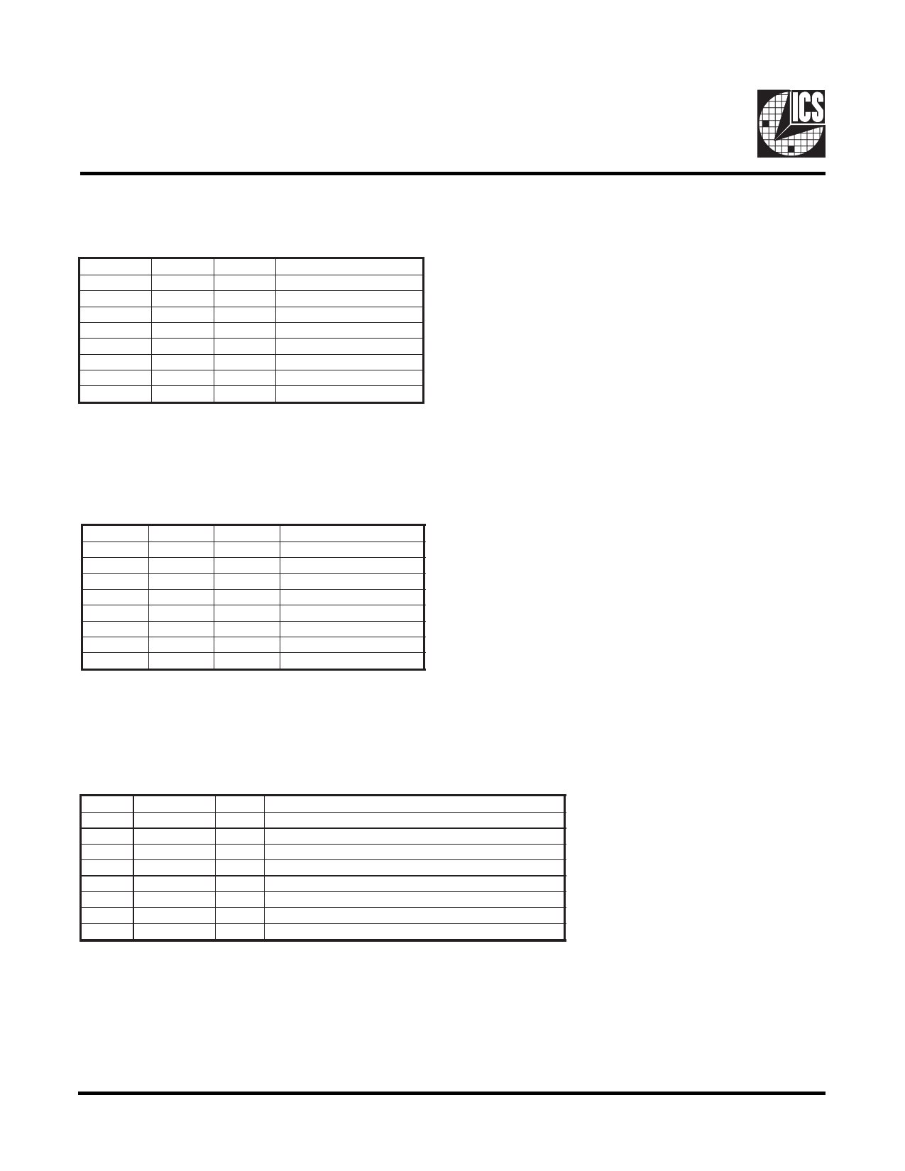
Byte 1: CPU, Active/Inactive Register (1 = enable, 0 = disable)
Bit
Bit 7
Bit 6
Bit 5
Bit 4
Bit 3
Bit 2
Bit 1
Bit 0
Pin #
-
46
-
-
39
42
43
45
PWD
1
1
1
1
1
1
1
1
Description
(Reserved)
CPUCLK_F (Act/Inact)
(Reserved)
(Reserved)
SDRAM_F (Act/Inact)
CPUCLK2 (Act/Inact)
CPUCLK1 (Act/Inact)
CPUCLK0 (Act/Inact)
Byte 2: PCI Active/Inactive Register (1 = enable, 0 = disable)
Bit
Bit 7
Bit 6
Bit 5
Bit 4
Bit 3
Bit 2
Bit 1
Bit 0
Pin #
7
18
17
13
12
11
10
8
PWD
1
1
1
1
1
1
1
1
Description
PCICLK_F (Act/Inact)
PCICLK6 (Act/Inact)
PCICLK5 (Act/Inact)
PCICLK4 (Act/Inact)
PCICLK3 (Act/Inact)
PCICLK2 (Act/Inact)
PCICLK1 (Act/Inact)
PCICLK0 (Act/Inact)
Byte 3: SDRAM Active/Inactive Register (1 = enable, 0 = disable)
Bit
Bit 7
Bit 6
Bit 5
Bit 4
Bit 3
Bit 2
Bit 1
Bit 0
Pin #
-
-
-
-
28
29
31
32
PWD
1
1
1
1
1
1
1
1
Description
(Reserved)
(Reserved)
(Reserved)
(Reserved)
SDRAM7 (Active/Inactive)
SDRAM6 (Active/Inactive)
SDRAM5 (Active/Inactive)
SDRAM4 (Active/Inactive)
Notes:
1. Inactive means outputs are held LOW and are disabled from switching.
2. Latched Frequency Selects (FS#) will be inverted logic load of the input frequency select pin conditions.
4