HD74LVC2G53 데이터 시트보기 (PDF) - Renesas Electronics
부품명
상세내역
일치하는 목록
HD74LVC2G53 Datasheet PDF : 12 Pages
| |||
HD74LVC2G53
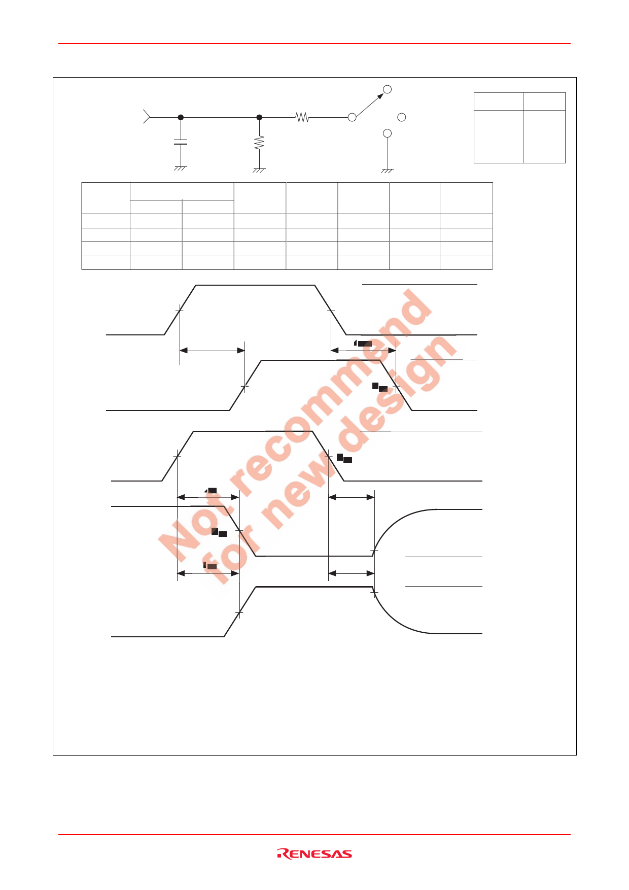
Test Circuit (cont.)
From Output
CL
Load circuit
RL
S1
VTT
OPEN
GND
RL
TEST
tPLH / tPHL
tZH / tHZ
tZL / tLZ
S1
OPEN
GND
VTT
VCC (V)
1.8±0.15
2.5±0.2
3.3±0.3
5.0±0.5
INPUTS
VI
VCC
VCC
VCC
VCC
tr / tf
≤ 2 ns
≤ 2 ns
≤ 2.5 ns
≤ 2.5 ns
Vref
VCC / 2
VCC / 2
VCC / 2
VCC / 2
VTT
2 × VCC
2 × VCC
2 × VCC
2 × VCC
CL
30 pF
30 pF
50 pF
50 pF
RL
1.0 kΩ
500 Ω
500 Ω
500 Ω
Input
Output
Vref
t PLH
Vref
Vref
t PHL
Vref
Control
Input
Vref
t ZL
Output
(Waveform – A)
Vref
t ZH
Output
(Waveform – B)
Vref
Vref
t LZ
VOL + ∆V
t HZ
VOH – ∆V
∆V
0.15 V
0.15 V
0.3 V
0.3 V
VI
0V
V OH
V OL
VI
0V
VOH
V OL
V OH
VOL
Notes: 1. CL includes probe and jig capacitance.
2. Waveform–A is for an output with internal conditions such that the output is low except
when disabled by the output control.
3. Waveform–B is for an output with internal conditions such that the output is high except
when disabled by the output control.
4. All input pulses are supplied by generators having the following characteristics:
PRR ≤ 10MHz, Zo = 50 Ω.
5. The output are measured one at a time with one transition per measurement.
Rev.3.00 Jul 07, 2005 page 8 of 11
Share Link: 