HD74BC540AFPEL 데이터 시트보기 (PDF) - Renesas Electronics
부품명
상세내역
일치하는 목록
HD74BC540AFPEL Datasheet PDF : 8 Pages
| |||
HD74BC540A
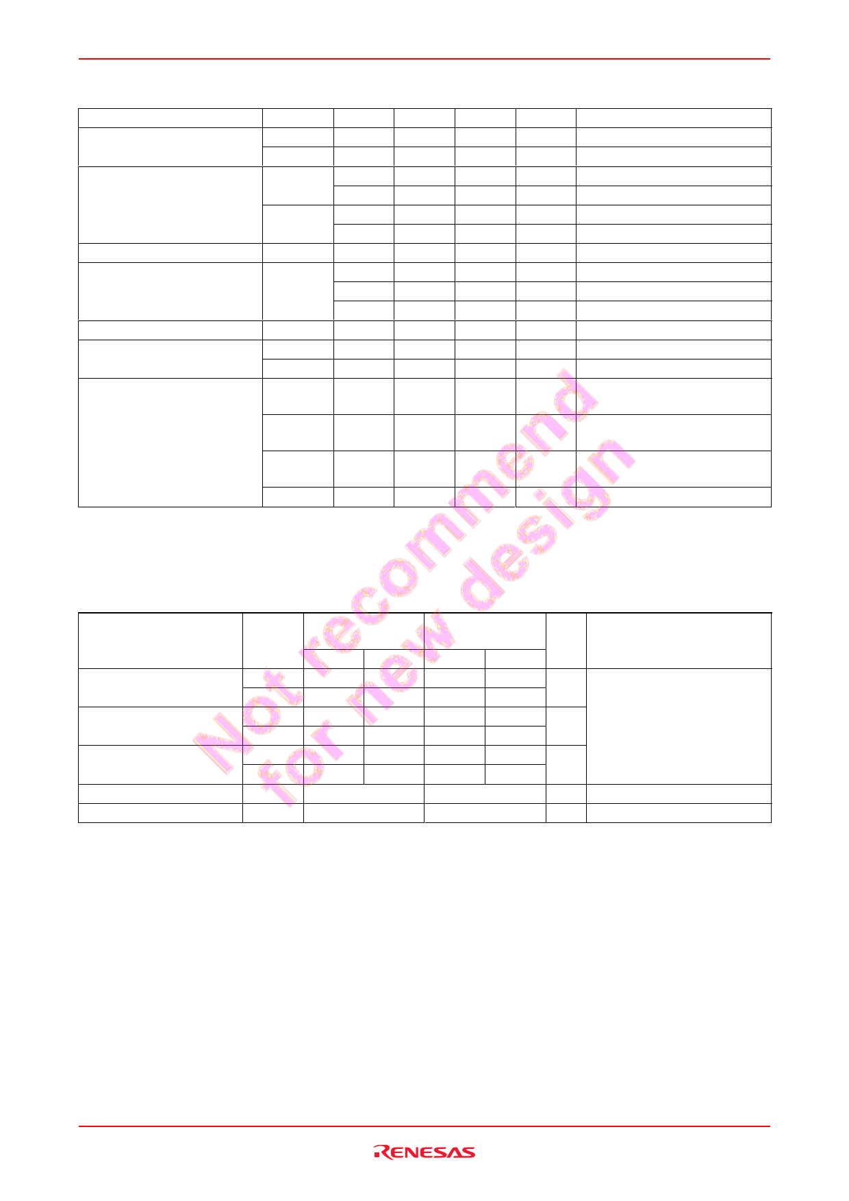
Electrical Characteristics (Ta = –40 to +85°C)
Item
Input voltage
Output voltage
Input diode voltage
Input current
Short circuit output current*1
Off state output current
Supply current
Symbol
VIH
VIL
VOH
VOL
VIK
II
IOS
IOZH
IOZL
ICCL
VCC(V)
4.5
4.5
4.5
4.5
4.5
5.5
5.5
5.5
5.5
5.5
5.5
5.5
Min
2.0
—
2.4
2.0
—
—
—
—
—
—
–100
—
—
—
Max
—
0.8
—
—
0.5
0.55
–1.2
–250
1.0
100
–225
50
–50
27.5
Unit
V
V
V
V
V
V
V
µA
µA
µA
mA
µA
µA
mA
Test Conditions
IOH = –3 mA
IOH = –15 mA
IOL = 48 mA
IOL = 64 mA
IIN = –18 mA
VIN = 0 V
VIN = 5.5 V
VIN = 7.0 V
VIN = 0 or 5.5 V
VO = 2.7 V
VO = 0.5 V
VIN = 0 or 5.5 V
All outputs is “L”
ICCH
5.5
—
2.5
mA
VIN = 0 or 5.5 V
All outputs is “H”
ICCZ
5.5
—
2.5
mA
VIN = 0 or 5.5 V
All outputs is “Z”
ICCT*2
5.5
—
1.5
mA
VIN = 3.4V or 0.5V
Notes: 1. Not more than one output should be shorted at a time and duration of the short circuit should not exceed one
second.
2. When input by the TTL level, it shows ICC increase at per one input pin.
Switching Characteristics (CL = 50 pF)
Item
Propagation delay time
Output enable time
Output disable time
Input capacitance
Output capacitance
Ta = 25°C
Symbol
VCC = 5.0 V
Min
Max
tPLH
3.0
6.0
tPHL
3.0
6.0
tZH
3.0
9.0
tZL
3.0
9.0
tHZ
3.0
8.0
tLZ
3.0
8.0
CIN
3.0(Typ)
CO
15.0(Typ)
Ta = –40 to +85°C
VCC = 5.0 V ±10
Min
Max
Unit
Test Conditions
3.0
7.0
ns See under figure
3.0
7.0
3.0
11.0
ns
3.0
11.0
3.0
10.0
ns
3.0
10.0
—
pF VIN = VCC or GND
—
pF VO = VCC or GND
Rev.2.00, Jul.16.2004, page 4 of 7
Share Link: 