EDI88512C 데이터 시트보기 (PDF) - White Electronic Designs Corporation
부품명
상세내역
일치하는 목록
EDI88512C Datasheet PDF : 7 Pages
| |||
White Electronic Designs
EDI88512C
ABSOLUTE MAXIMUM RATINGS
Parameter
Voltage on any pin relative to Vss
Operating Temperature TA (Ambient)
Commercial
Industrial
Military
Storage Temperature, Plastic
Power Dissipation
Output Current
Junction Temperature, TJ
Value
Unit
-0.5 to 7.0
V
0 to +70
°C
-40 to +85
°C
-55 to +125
°C
-65 to +150
°C
1
W
20
mA
175
°C
NOTE:
Stress greater than those listed under “Absolute Maximum Ratings” may cause
permanent damage to the device. This is a stress rating only and functional operation
of the device at these or any other conditions greater than those indicated in the
operational sections of this specification is not implied. Exposure to absolute maximum
rating conditions for extended periods may affect reliability.
TRUTH TABLE
OE# CS# WE#
Mode
Output
X
H
X
Standby
High Z
H
L
H Output Deselect High Z
L
L
H
Read
Data Out
X
L
L
Write
Data In
Power
ICC2, ICC3
ICC1
ICC1
ICC1
RECOMMENDED OPERATING CONDITIONS
Parameter
Supply Voltage
Supply Voltage
Input High Voltage
Input Low Voltage
Symbol Min
VCC
4.5
VSS
0
VIH
2.2
VIL
-0.3
Typ
Max
Unit
5.0
5.5
V
0
0
V
— VCC +0.5 V
—
+0.8
V
CAPACITANCE
TA = +25°C
Parameter Symbol
Condition
Max Unit
Address Lines
CI
VIN = Vcc or Vss, f = 1.0MHz 12 pF
Data Lines
CO VOUT = Vcc or Vss, f = 1.0MHz 14 pF
These parameters are sampled, not 100% tested.
Parameter
Input Leakage Current
Output Leakage Current
Operating Power Supply Current
Standby (TTL) Power Supply Current
Full Standby Power Supply Current
Symbol
ILI
ILO
ICC1
ICC2
ICC3
Output Low Voltage
VOL
Output High Voltage
VOH
NOTE: DC test conditions: Vil = 0.3V, Vih = Vcc -0.3V
DC CHARACTERISTICS
VCC = 5V, -55°C ≤ *TA ≤ +125°C
Conditions
VIN = 0V to VCC
VI/O = 0V to VCC
WE#, CS# = VIL, II/O = 0mA, Min Cycle (70-100ns)
CS# ≥ VIH, VIN ≤ VIL, VIN ≥ VIH
CS# ≥ VCC -0.2V
C
VIN ≥ Vcc -0.2V or VIN ≤ 0.2V
LP
IOL = 2.1mA
IOH = -1.0mA
Min Typ* Max Units
—
—
±10
µA
—
—
±10
µA
—
45
75
mA
—
3
10
mA
—
—
5
mA
—
—
2
mA
—
—
0.4
V
2.4
—
—
V
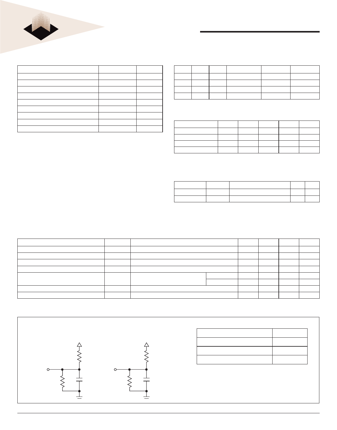
AC TEST CONDITIONS
Figure 1
Vcc
Figure 2
Q
255Ω
480Ω
30pF
Q
255Ω
Vcc
480Ω
5pF
Input Pulse Levels
VSS to 3.0V
Input Rise and Fall Times
5ns
Input and Output Timing Levels
1.5V
Output Load
Figure 1
NOTE: For tEHQZ, tGHQZ and tWLQZ, CL = 5pF Figure 2
White Electronic Designs Corp. reserves the right to change products or specifications without notice.
February 2001
Rev. 11
2
White Electronic Designs Corporation • (602) 437-1520 • www.wedc.com
Share Link: 