DG506A 데이터 시트보기 (PDF) - Intersil
부품명
상세내역
일치하는 목록
DG506A Datasheet PDF : 19 Pages
| |||
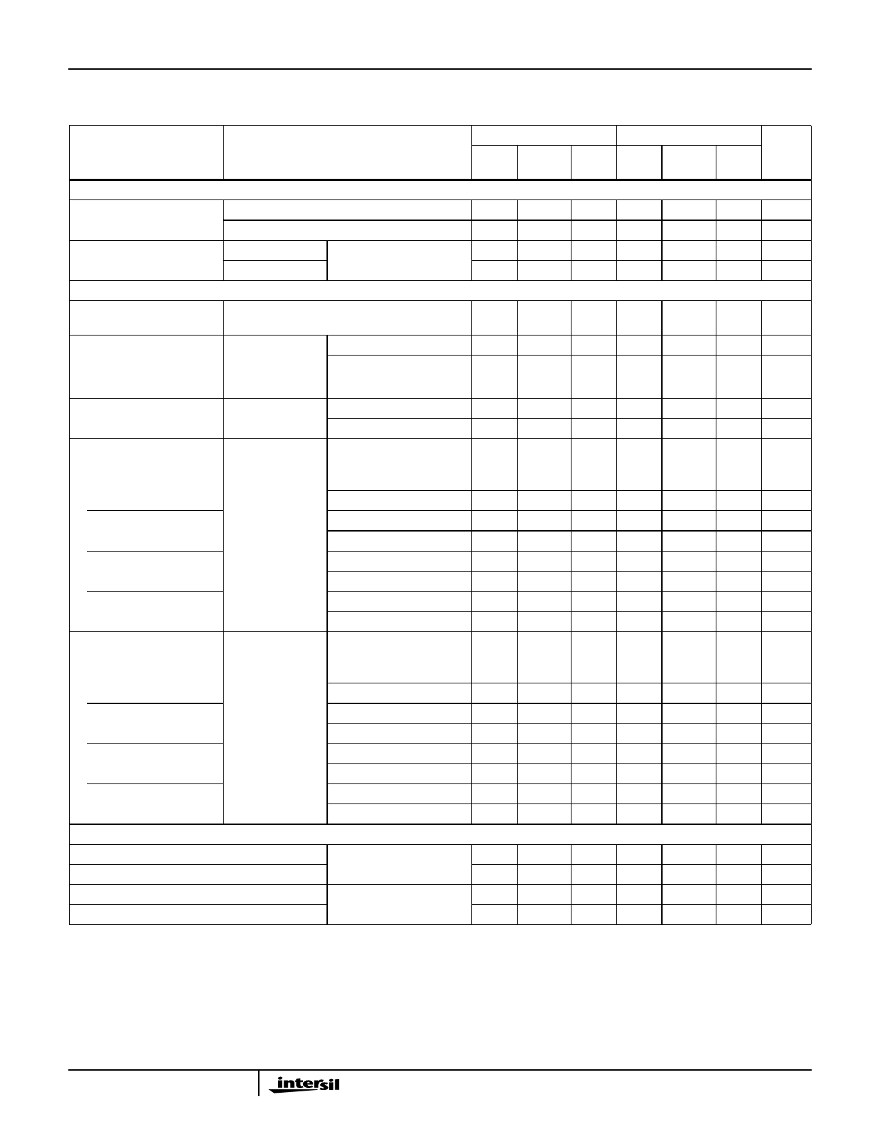
DG506A, DG507A, DG508A, DG509A
Electrical Specifications TA = Over Operating Temperature Range, V+ = +15V, V- = -15V, GND = 0V, VEN = 2.4V,
Unless Otherwise Specified
“A” SUFFIX
“B” AND “C” SUFFIX
PARAMETER
TEST CONDITIONS
(NOTE 3)
(NOTE 3)
MIN TYP MAX MIN TYP MAX UNITS
DIGITAL INPUT CHARACTERISTICS
Address Input Current, Input VA = 2.4V
Voltage High, IAH
VA = 15V
Address Input Current Input VEN = 2.4V
Voltage Low, IAL
VEN = 0V
ANALOG SWITCH CHARACTERISTICS
VA = 0V
-30
-
-
-
-
-
µA
-
-
30
-
-
-
µA
-30
-
-
-
-
-
µA
-30
-
-
-
-
-
µA
Analog Signal Range,
VANALOG
(Note 7)
-15
-
+15
-
-
-
V
Drain-Source ON
Resistance, rDS(ON)
Sequence Each IS = -200µA, VD = +10V
-
-
500
-
-
-
Ω
Switch ON
VAL = 0.8V
IS = -200µA, VD = -10V
-
-
500
-
-
-
Ω
VAH = 2.4V
Source OFF Leakage
Current, IS(OFF)
VEN = 0V
VS = +10V, VD = -10V
-
-
50
-
-
-
nA
VS = -10V, VD = +10V
-50
-
-
-
-
-
nA
Drain OFF Leakage Current, VEN = 0V
ID(OFF)
DG506A
VS = -10V, VD = +10V
-
-
300
-
-
-
nA
VS = +10V, VD = -10V
-300
-
-
-
-
-
nA
DG507A
VS = -10V, VD = +10V
-
-
200
-
-
-
nA
VS = +10V, VD = -10V
-200
-
-
-
-
-
nA
DG508A
VS = -10V, VD = +10V
-
-
200
-
-
-
nA
VS = +10V, VD = -10V
-200
-
-
-
-
-
nA
DG509A
VS = -10V, VD = +10V
-
-
100
-
-
-
nA
VS = +10V, VD = -10V
-100
-
-
-
-
-
nA
Drain ON Leakage Current, (Note 6)
ID(ON)
DG506A
DG507A
Sequence Each
Switch ON
VD = VS(ALL) = +10V
-
-
300
-
-
-
nA
VAL = 0.8V
VAH = 2.4V
VD = VS(ALL) = -10V
-300
-
-
-
-
-
nA
VD = VS(ALL) = +10V
-
-
200
-
-
-
nA
VD = VS(ALL) = -10V
-200
-
-
-
-
-
nA
DG508A
VD = VS(ALL) = +10V
-
-
200
-
-
-
nA
VD = VS(ALL) = -10V
-200
-
-
-
-
-
nA
DG509A
VD = VS(ALL) = +10V
-
-
100
-
-
-
nA
VD = VS(ALL) = -10V
-100
-
-
-
-
-
nA
POWER SUPPLY CHARACTERISTICS
Positive Supply Current, I+
Negative Supply Current, I-
VEN = 5.0V, VA = 0V
-3.2
-
4.5
-
-
-3.2
-
4.5
-
-
-
mA
-
mA
Positive Standby Supply Current, I+
Negative Standby Supply Current, I-
VEN = 0V, VA = 0V
-3.2
-
4.5
-
-
-
mA
-3.2
-
4.5
-
-
-
mA
NOTES:
3. Typical values are for design aid only, not guaranteed and not subject to production testing.
4. The algebraic convention whereby the most negative value is a minimum, and the most positive value is a maximum, is used in this data sheet.
5. Off isolation = 20Log |VS|/|VD|, where VS = input to Off switch, and VD = output due to VS.
6. ID(ON) is leakage from driver into “ON” switch.
7. Parameter not tested. Parameter guaranteed by design or characterization.
6
Share Link: 