CD4001 데이터 시트보기 (PDF) - Fairchild Semiconductor
부품명
상세내역
일치하는 목록
CD4001
Fairchild Semiconductor

CD4001 Datasheet PDF : 9 Pages
| |||
Absolute Maximum Ratings(Note 1)
(Note 2)
Voltage at any Pin
Power Dissipation (PD)
Dual-In-Line
Small Outline
VDD Range
Storage Temperature (TS)
Lead Temperature (TL)
(Soldering, 10 seconds)
−0.5V to VDD +0.5V
700 mW
500 mW
−0.5 VDC to +18 VDC
−65°C to +150°C
260°C
Recommended Operating
Conditions
Operating Range (VDD)
Operating Temperature Range
3 VDC to 15 VDC
CD4001BC, CD4011BC
−55°C to +125°C
Note 1: “Absolute Maximum Ratings” are those values beyond which the
safety of the device cannot be guaranteed. Except for “Operating Tempera-
ture Range” they are not meant to imply that the devices should be oper-
ated at these limits. The Electrical Characteristics tables provide conditions
for actual device operation.
Note 2: All voltages measured with respect to VSS unless otherwise speci-
fied.
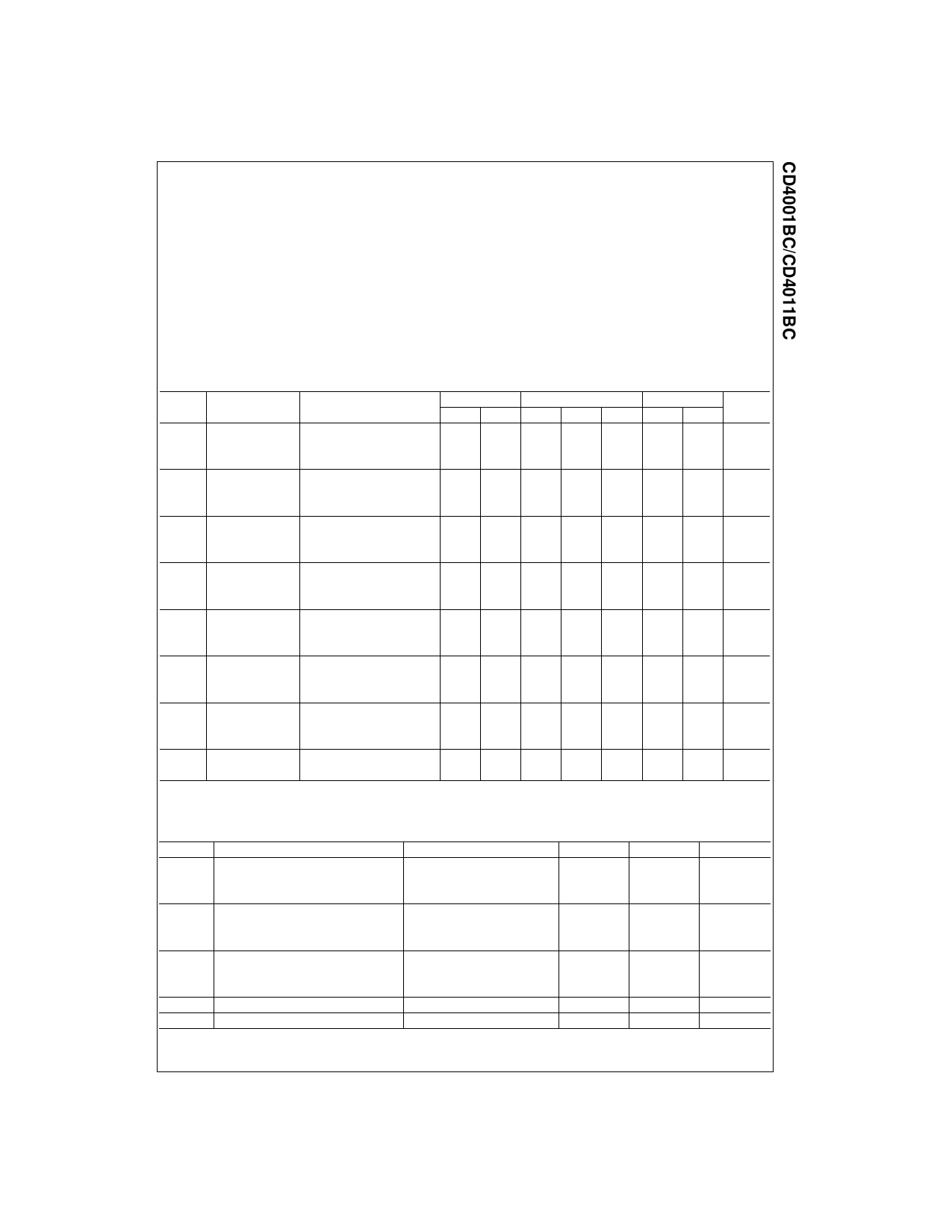
DC Electrical Characteristics (Note 2)
Symbol
Parameter
Conditions
IDD
Quiescent Device VDD = 5V, VIN = VDD or VSS
Current
VDD = 10V, VIN = VDD or VSS
VDD = 15V, VIN = VDD or VSS
VOL
LOW Level
VDD = 5V
Output Voltage
VDD = 10V |IO| < 1 µA
VDD = 15V
VOH
HIGH Level
VDD = 5V
Output Voltage
VDD = 10V |IO| < 1 µA
VDD = 15V
VIL
LOW Level
VDD = 5V, VO = 4.5V
Input Voltage
VDD = 10V, VO = 9.0V
VDD = 15V, VO = 13.5V
VIH
HIGH Level
VDD = 5V, VO = 0.5V
Input Voltage
VDD = 10V, VO = 1.0V
VDD = 15V, VO = 1.5V
IOL
LOW Level Output VDD = 5V, VO = 0.4V
Current
VDD = 10V, VO = 0.5V
(Note 3)
VDD = 15V, VO = 1.5V
IOH
HIGH Level Output VDD = 5V, VO = 4.6V
Current
VDD = 10V, VO = 9.5V
(Note 3)
VDD = 15V, VO = 13.5V
IIN
Input Current
VDD = 15V, VIN = 0V
VDD = 15V, VIN = 15V
Note 3: IOL and IOH are tested one output at a time.
−55°C
Min Max
0.25
0.5
1.0
0.05
0.05
0.05
4.95
9.95
14.95
1.5
3.0
4.0
3.5
7.0
11.0
0.64
1.6
4.2
−0.64
−1.6
−4.2
−0.10
0.1
Min
4.95
9.95
14.95
3.5
7.0
11.0
0.51
1.3
3.4
−0.51
−1.3
−3.4
+25°C
Typ
0.004
0.005
0.006
0
0
0
5
10
15
2
4
6
3
6
9
0.88
2.25
8.8
−0.88
−2.25
−8.8
−10−5
10−5
Max
0.25
0.50
1.0
0.05
0.05
0.05
1.5
3.0
4.0
−0.10
0.10
+125°C
Min Max
7.5
15
30
0.05
0.05
0.05
4.95
9.95
14.95
1.5
3.0
4.0
3.5
7.0
11.0
0.36
0.9
2.4
−0.36
−0.9
−2.4
−1.0
1.0
Units
µA
V
V
V
V
mA
mA
µA
AC Electrical Characteristics (Note 4)
CD4001BC: TA = 25°C, Input tr; tf = 20 ns. CL = 50 pF, RL = 200k. Typical temperature coefficient is 0.3%/°C.
Symbol
Parameter
Conditions
Typ
Max
tPHL
Propagation Delay Time,
VDD = 5V
HIGH-to-LOW Level
VDD = 10V
VDD = 15V
tPLH
Propagation Delay Time,
VDD = 5V
LOW-to-HIGH Level
VDD = 10V
VDD = 15V
tTHL, tTLH Transition Time
VDD = 5V
VDD = 10V
VDD = 15V
CIN
Average Input Capacitance
Any Input
CPD
Power Dissipation Capacity
Any Gate
Note 4: AC Parameters are guaranteed by DC correlated testing.
120
250
50
100
35
70
110
250
50
100
35
70
90
200
50
100
40
80
5
7.5
14
Units
ns
ns
ns
pF
pF
3
www.fairchildsemi.com
Share Link: