PI74FCT374CTLE 데이터 시트보기 (PDF) - Pericom Semiconductor
부품명
상세내역
일치하는 목록
PI74FCT374CTLE Datasheet PDF : 9 Pages
| |||
PI74FCT374T
PI74FCT574T
1122334455667788990011223344556677889900112233445566778899001122112233445566778899001122334455667788990011223344556677889900112211223344556677889900112233445566778899001122334455667788990011221122334455667788O9900c1122t33a44l5566D778899R0011e2233g44i55s6677t88e99r00s1122(1132233-44S5566t77a88t99e0011)22
Maximum Ratings
(Above which the useful life may be impaired. For user guidelines, not tested.)
Storage Temperature ................................................................. –65°C to +150°C
Ambient Temperature with Power Applied ................................. -40°C to +85°C
Supply Voltage to Ground Potential (Inputs & Vcc Only) .......... –0.5V to +7.0V
Supply Voltage to Ground Potential (Outputs & D/O Only) ....... –0.5V to +7.0V
DC Input Voltage ......................................................................... –0.5V to +7.0V
DC Output Current ................................................................................... 120 mA
Power Dissipation ......................................................................................... 0.5W
Note:
Stresses greater than those listed under MAXI-
MUM RATINGS may cause permanent damage to
the device. This is a stress rating only and functional
operation of the device at these or any other
conditions above those indicated in the operational
sections of this specification is not implied.
Exposure to absolute maximum rating conditions for
extended periods may affect reliability.
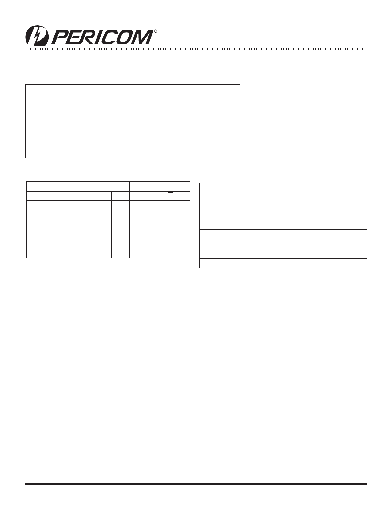
Truth Table(1)
Inputs
Outputs Internal
Function
OE CP DN
ON
QN
High-Z
H
LX
Z
NC
H
HX
Z
NC
Load Register L
↑L
L
H
L
↑H
H
L
H
↑L
Z
H
H
↑H
Z
L
1. H = High Voltage Level
L = Low Voltage Level
X = Don’t Care
Z = High Impedance
NC = No Change
↑= LOW-to-HIGH transition
Pin Description
Pin Name
OE
CP
D0-D7
O0-O7
O0-O7
GND
VCC
Description
Output Enable Input (Active LOW)
Clock Pulse for the register. Enters data on
LOW-to-HIGH transition
Data Inputs
3-State Outputs (true)
3-State Outputs (inverted)
Ground
Power
2
PS2016C 10/01/04
Share Link: 