PI49FCT807ATS 데이터 시트보기 (PDF) - Pericom Semiconductor
부품명
상세내역
일치하는 목록
PI49FCT807ATS Datasheet PDF : 7 Pages
| |||
PI49FCT807/2807T
Fast CMOS Clock Driver
12345678901234567890123456789012123456789012345678901234567890121234567890123456789012345678901212345678901234567890123456789012123456789012
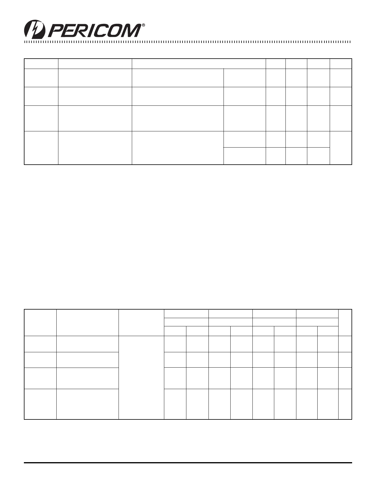
Power Supply Characteristics
Parameters Description
Test Conditions(1)
Min. Typ.(2) Max. Units
ICC
Quiescent Power
Supply Current
VCC = Max.
VIN = GND
or Vcc
3
30
µA
∆ICC
Supply Current per
Input @ TTL HIGH
VCC = Max.,
VIN = 3.4V(3)
0.5 1.5 mA
ICCD
Supply Current per
VCC = Max., Outputs Open
VIN = VCC
0.4
Input per MHz(4)
50% Duty Cycle,
VIN = GND
One Input Toggling
IC
Total Power Supply
VCC = Max., Outputs Open
VIN = VCC
20
Current(6)
fCP = 50 MHZ,
VIN = GND
50% Duty Cycle
VIN = 3.4V
20.7
VIN = GND
Notes:
1. For Max. or Min. conditions, use appropriate value specified under Electrical Characteristics for the applicable device.
2. Typical values are at Vcc = 5.0V, +25°C ambient.
3. Per TTL driven input (VIN = 3.4V); all other inputs at Vcc or GND.
4. This parameter is not directly testable, but is derived for use in Total Power Supply Calculations.
5. Values for these conditions are examples of the Icc formula. These limits are guaranteed but not tested.
6. IC =IQUIESCENT + IINPUTS + IDYNAMIC
IC = ICC + ∆ICC DHNT + ICCD (fCP/2 + fINI)
ICC = Quiescent Current
∆ICC = Power Supply Current for a TTL High Input (VIN = 3.4V)
DH = Duty Cycle for TTL Inputs High
NT = Number of TTL Inputs at DH
ICCD = Dynamic Current Caused by an Input Transition Pair (HLH or LHL)
fCP = Clock Frequency for Register Devices (Zero for Non-Register Devices)
fI = Input Frequency
NI = Number of Inputs at fI
All currents are in milliamps and all frequencies are in megahertz.
0.6 mA/
MHz
30(5) mA
33(5)
Switching Characteristics over Operating Range
Parameters Description
Conditions(1)
807/2807T
Com.
Min. Max.
tPLH
tPHL
tSK(o)
tSK(p)
tSK(t)
Propagation Delay
A TO BN
Skew between two outputs
of same package(3)
Skew between opposite
transitions of same
output (|tPHL — tPLH|)(3)
Skew between outputs of
different package at same
power supply, temperature
and speed grade(3)
CL = 50pF
RL = 500Ω
1.5
4.5
—
0.5
—
0.5
—
1.0
Notes:
1. See test circuit and wave forms.
2. Minimum limits are guaranteed but not tested on Propagation Delays.
3. This parameter is guaranteed but not tested.
807AT
Com.
Min. Max.
1.5
4.0
—
0.5
—
0.5
—
1.0
807BT
Com.
Min. Max.
1.5
3.8
—
0.35
—
0.35
—
0.75
807CT
Com.
Min. Max. Units
1.5
3.5 ns
— 0.25 ns
— 0.35 ns
— 0.75 ns
3
PS7008D 09/24/04
Share Link: 