PI74FCT163240A 데이터 시트보기 (PDF) - Pericom Semiconductor
부품명
상세내역
일치하는 목록
PI74FCT163240A Datasheet PDF : 5 Pages
| |||
PI74FCT163240
12345678901234567890123456789012123456789012345678901234567890121234567890123456789012345678901212334.5367V89011623-4B56i7t8B901u2f3f4e56r7/8L90i1n21e23D45r67iv89e0r12
Maximum Ratings
(Above which the useful life may be impaired. For user guidelines, not tested.)
Storage Temperature ............................................................. –65°C to +150°C Note:
1
Ambient Temperature with Power Applied ............................ –40°C to +85°C
Supply Voltage to Ground Potential (Inputs & Vcc Only) ...... –0.5V to +7.0V
Supply Voltage to Ground Potential (Outputs & D/O Only) .. –0.5V to +7.0V
Stresses greater than those listed under MAXIMUM
2 RATINGS may cause permanent damage to the de-
vice. This is a stress rating only and functional opera-
tion of the device at these or any other conditions
DC Input Voltage .................................................................... –0.5V to +7.0V
DC Output Current .............................................................................. 120 mA
Power Dissipation .................................................................................... 1.0W
above those indicated in the operational sections of
3 this specification is not implied. Exposure to absolute
maximum rating conditions for extended periods
may affect reliability.
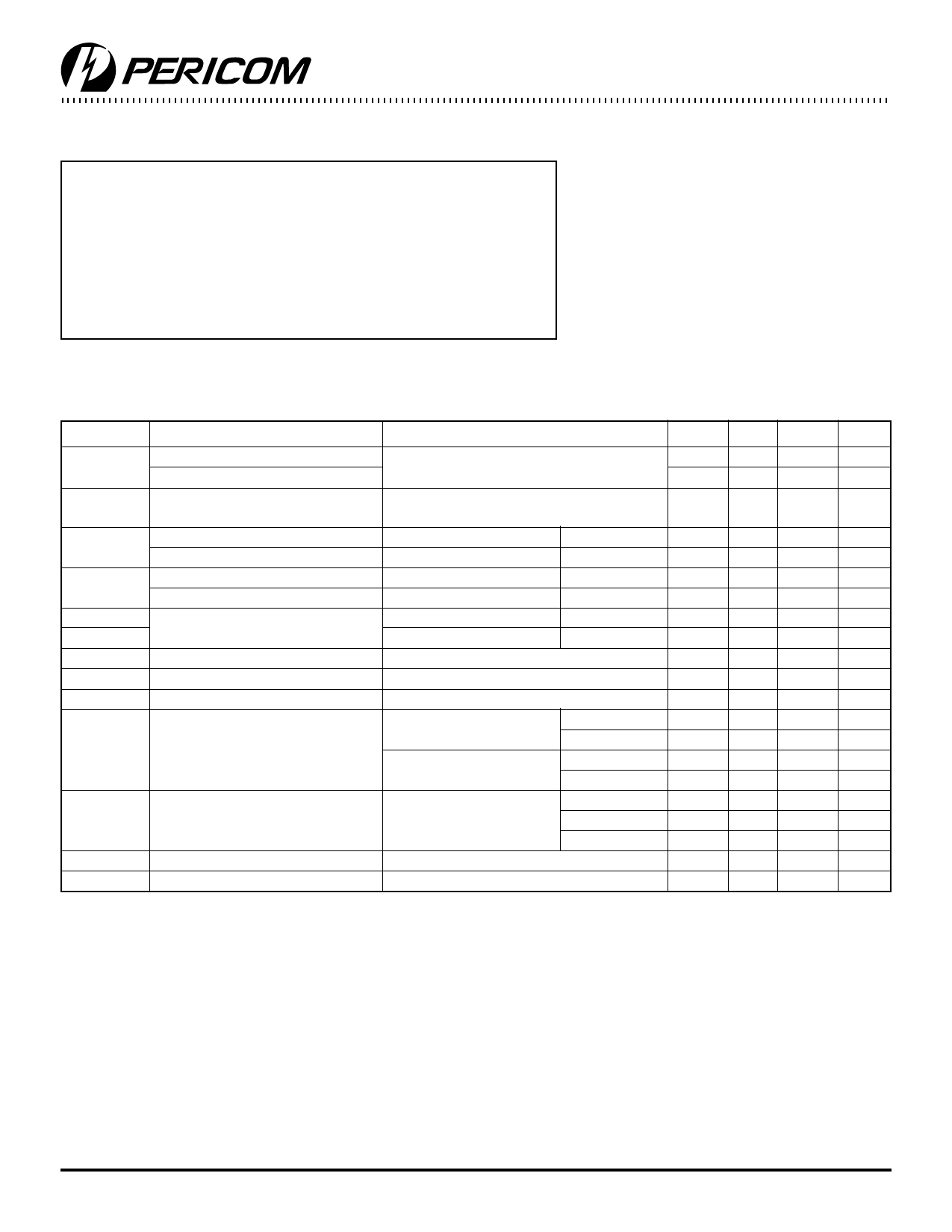
DC Electrical Characteristics (Over the Operating Range, TA = –40°C to +85°C, VCC = 2.7V to 3.6V)
Parameters
Description
Test Conditions(1)
Min. Typ.(2) Max. Units
VIH
VIL
IIH
IIL
IOZH
IOZL
VIK
IODH
IODL
VOH
VOL
IOS
VH
Input HIGH Voltage (Input pins)
Input HIGH Voltage (I/O pins)
Input LOW Voltage
(Input and I/O pins)
Input HIGH Current (Input pins)
Input HIGH Current (I/O pins)
Input LOW Current (Input pins)
Input LOW Current (I/O pins)
High Impedance Output Current
(3-State Output pins)
Clamp Diode Voltage
Output HIGH Current
Output LOW Current
Output HIGH Voltage
Output LOW Voltage
Short Circuit Current(4)
Input Hysteresis
Guaranteed Logic HIGH Level
Guaranteed Logic LOW Level
2.2 — 5.5 V
2.0 — Vcc+0.5 V
–0.5 — 0.8 V
VCC = Max.
VIN = 5.5V
— — ±1 µA
VCC = Max.
VIN = VCC
— — ±1 µA
VCC = Max.
VIN = GND
— — ±1 µA
VCC = Max.
VIN = GND
— — ±1 µA
VCC = Max.
VOUT = VCC
—
—
±1
µA
VCC = Max.
VOUT = GND —
—
±1
µA
VCC = Min., IIN = –18 mA
— –0.7 –1.2 V
VCC = 3.3V, VIN = VIH or VIL, VO = 1.5V(3) –36 –60 –110 mA
VCC = 3.3V, VIN = VIH or VIL, VO = 1.5V(3) 50
90 200 mA
VCC = Min.
IOH = –0.1 mA Vcc-0.2 —
—
V
VIN = VIH or VIL
IOH = –3 mA 2.4 3.0 —
V
VCC = 3.0V,
IOH = –8 mA 2.4(5) 3.0
—
V
VIN = VIH OR VIL
IOH = –24 mA 2.0 —
—
V
VCC = Min.
IOL = 0.1 mA —
—
0.2
V
VIN = VIH or VIL
IOL = 16 mA
—
0.2 0.4
V
IOL = 24 mA
—
0.3 0.5
V
VCC = Max.(3), VOUT = GND
–60 –85 –240 mA
— 150 — mV
Notes:
1. For Max. or Min. conditions, use appropriate value specified under Electrical Characteristics for the applicable device type.
2. Typical values are at Vcc = 3.3V, +25°C ambient and maximum loading.
3. Not more than one output should be shorted at one time. Duration of the test should not exceed one second.
4. This parameter is guaranteed but not tested.
5. VOH = VCC – 0.6V at rated current.
4
5
6
7
8
9
10
11
12
13
14
15
3
PS2051A 01/20/97
Share Link: 