ADT7411ARQZ10 데이터 시트보기 (PDF) - Analog Devices
부품명
상세내역
일치하는 목록
ADT7411ARQZ10
Analog Devices

ADT7411ARQZ10 Datasheet PDF : 36 Pages
| |||
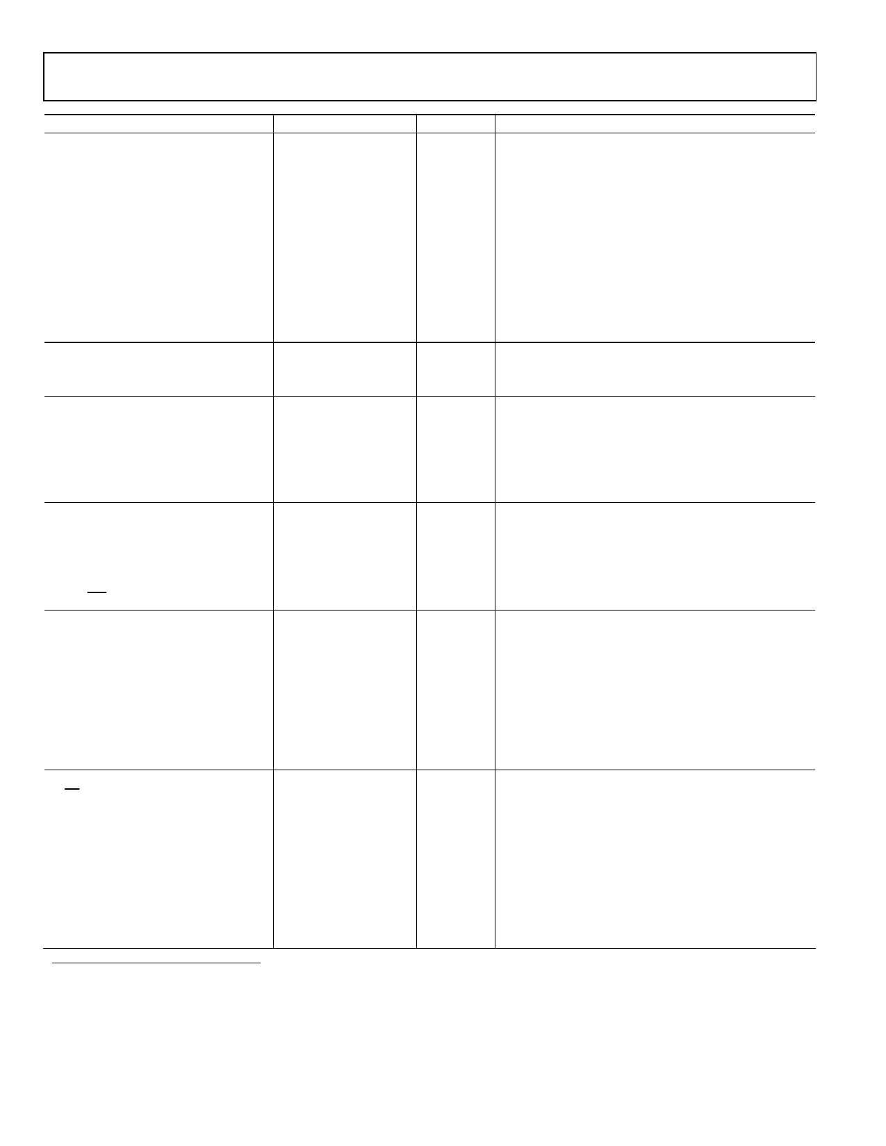
ADT7411
Parameter1
ROUND ROBIN UPDATE RATE2
Slow ADC @ 25°C
Averaging On
Averaging Off
Averaging On
Averaging Off
Fast ADC @ 25°C
Averaging On
Averaging Off
Averaging On
Averaging Off
ON-CHIP REFERENCE3
Reference Voltage
Temperature Coefficient
DIGITAL INPUTS1, 3
Input Current
VIL, Input Low Voltage
VIH, Input High Voltage
Pin Capacitance
SCL, SDA Glitch Rejection
DIGITAL OUTPUT
Output High Voltage, VOH
Output Low Voltage, VOL
Output High Current, IOH
Output Capacitance, COUT
INT/INT Output Saturation Voltage
I2C TIMING CHARACTERISTICS4, 5
Serial Clock Period, t1
Data In Setup Time to SCL High, t2
Data Out Stable after SCL Low, t3
SDA Low Setup Time to SCL Low
(Start Condition), t4
SDA High Hold Time after SCL High
(Stop Condition), t5
SDA and SCL Fall Time, t6
SPI TIMING CHARACTERISTICS1, 3, 6
CS to SCLK Setup Time, t1
SCLK High Pulse Width, t2
SCLK Low Pulse Width, t3
Data Access Time after SCLK
Falling Edge, t4 6
Data Setup Time Prior to SCLK
Rising Edge, t5
Data Hold Time after SCLK
Rising Edge, t6
Min Typ Max
125.4
17.1
140.36
12.11
9.26
578.96
24.62
3.25
2.25
80
±1
0.8
1.89
3
10
50
2.4
0.4
1
50
0.8
2.5
50
0
50
50
90
0
50
50
35
20
0
Unit
ms
ms
ms
ms
ms
µs
ms
ms
V
ppm/°C
µA
V
V
pF
ns
V
V
mA
pF
V
µs
ns
ns
ns
ns
ns
ns
ns
ns
ns
ns
ns
Conditions/Comments
Time to complete one measurement cycle through all
channels.
AIN1 and AIN2 are selected on Pins 7 and 8.
AIN1 and AIN2 are selected on Pins 7 and 8.
D+ and D– are selected on Pins 7 and 8.
D+ and D− are selected on Pins 7 and 8.
AIN1 and AIN2 are selected on Pins 7 and 8.
AIN1 and AIN2 are selected on pins 7 and 8.
D+ and D− are selected on Pins 7 and 8.
D+ and D− are selected on Pins 7 and 8.
VIN = 0 V to VDD.
All Digital Inputs.
Input filtering suppresses noise spikes of less than 50 ns.
ISOURCE = ISINK = 200 µA.
IOL = 3 mA.
VOH = 5 V.
IOUT = 4 mA.
Fast-Mode I2C. See Figure 2.
See Figure 2.
See Figure 2.
See Figure 2.
See Figure 2.
See Figure 3.
See Figure 3.
See Figure 3.
See Figure 3.
See Figure 3.
See Figure 3.
2 Round robin is the continuous sequential measurement of the following channels: VDD, internal temperature, external temperature (AIN1, AIN2), AIN3, AIN4, AIN5,
AIN6, AIN7, and AIN8.
3 Guaranteed by design and characterization, not production tested.
4 The SDA and SCL timing is measured with the input filters turned on so as to meet the FAST-Mode I2C specification. Switching off the input filters improves the transfer
rate, but has a negative effect on the EMC behavior of the part.
5 Guaranteed by design. Not tested in production.
6 All input signals are specified with tr = tf = 5 ns (10% to 90% of VDD), and timed from a voltage level of 1.6 V.
Rev. A | Page 4 of 36
Share Link: