A705 데이터 시트보기 (PDF) - ADDtek Corp
부품명
상세내역
일치하는 목록
A705 Datasheet PDF : 7 Pages
| |||
ABSOLUTE MAXIMUM RATINGS (Note)
Input Voltage, VDD
Output Voltage, VOUT
Maximum Junction Temperature, TJ
Storage Temperature Range
Lead Temperature (Soldering, 10 seconds)
Note: Exceeding these ratings could cause damage to the device. All voltages are with respect to Ground.
Currents are positive into, negative out of the specified terminal.
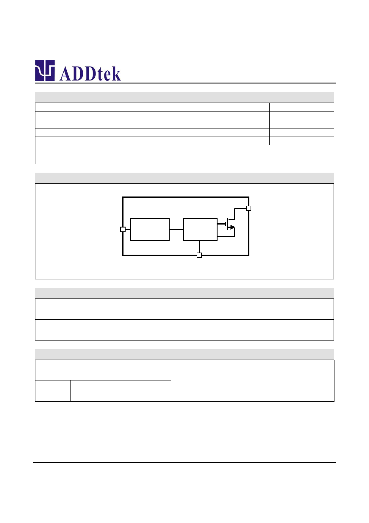
BLOCK DIAGRAM
A705
-0.3V to 13.2V
-0.3V to 17V
150°C
-40°C to 150°C
260°C
A705
VDD
Band-gap
Reference
Control
Circuit
GND
OUT
Pin Name
VDD
OUT
GND
PIN DESCRIPTION
Pin Function
Power supply.
Output pins. Connected to load.
Ground.
Package
N
SOT-89
S
TO-252
THERMAL RESISTANCE
θJT (°C /W)
35
7
Note:
TJ = TC + (PD × θJT)
θJT: Thermal Resistance - Junction to Tab.
TC: Case (Tab) Temperature.
TJ: Junction Temperature.
PD: Power Consumption.
Copyright © 2007 ADDtek Corp.
2
DD077_A -- AUGUST 2007
Share Link: 